Continue to Site

Welcome to EDAboard.com

Welcome to our site! EDAboard.com is an international Electronics Discussion Forum focused on EDA software, circuits, schematics, books, theory, papers, asic, pld, 8051, DSP, Network, RF, Analog Design, PCB, Service Manuals... and a whole lot more! To participate you need to register. Registration is free. Click here to register now.

[SOLVED] KiCad: How to get rid of "soldermask expose on trace" error?

Status
Not open for further replies.

pcsandhya82

Member level 3
Joined
Jul 31, 2010
Messages
58
Helped
0
Reputation
0
Reaction score
0
Trophy points
1,286
Location
Bangalore
Activity points
1,732
Hello all,

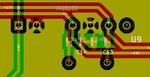
I have made a PCB with soldermask clearance as 0(Dimensions-> Pads Mask Clearance-> 0) , but the fabrication people has sent it back saying "We found soldermask expose on trace on both circuit layer" . Why does this happen? Ive attached snippets of my PCB where the Fab ppl points out this problem.


Thanks.
 

Attachments

  • snippet1.jpeg
    snippet1.jpeg
    41.8 KB · Views: 116
  • snippet2.jpeg
    snippet2.jpeg
    53.3 KB · Views: 125
  • snippet3.jpeg
    snippet3.jpeg
    77.6 KB · Views: 124
  • snippet4.jpeg
    snippet4.jpeg
    73 KB · Views: 115

You may have an orphan track on pin 5 which is throwing the error. It must be in the Gerber file so they will have detected it as a track crossing or intruding into a hole.

If that doesn't explain it, tell us what version of Kicad you are using, the latest is BZR5101 I think but the latest versions may only be available in Linux at the moment. If you are using the Windows or OSX versions you can build the latest version from source code.

Brian.
 

Hello,

I found the issue. It was with the design of footprint. there was an un necessary mask clearance given in the foot print which had to be removed.

Thanks.
 

Status
Not open for further replies.

Part and Inventory Search

Welcome to EDABoard.com

Sponsor

Back
Top