Continue to Site

Welcome to EDAboard.com

Welcome to our site! EDAboard.com is an international Electronics Discussion Forum focused on EDA software, circuits, schematics, books, theory, papers, asic, pld, 8051, DSP, Network, RF, Analog Design, PCB, Service Manuals... and a whole lot more! To participate you need to register. Registration is free. Click here to register now.

bias circuitry for protection diodes

Status
Not open for further replies.

mburakbaran

Member level 2
Joined
Jan 18, 2010
Messages
44
Helped
0
Reputation
0
Reaction score
0
Trophy points
1,286
Location
leuven
Activity points
1,724
Hello,

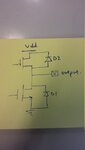
I'm working on EMI-robust digital drivers. I have a push pull output. I'd like to protect my output transistors in case a negative voltage appears on output (NMOS is in danger, body diode turns on an excessive current flowa) and in case a more than supply voltage appears on the output (this time PMOS is in danger).

I was thinking maybe biasing these diodes beforehand could help turning on them sooner before the body diodes does. In the schematic, for example 0.7V bias for the anode of D1 and 4.3V bias for the cathode of D2 seems to be helping a lot in case of an excessive EMI injection. Everything seems fine when I use VDC from cadence for the biases but I was wondering how to realize this. I must also mention that I need a wide bandwidth (upto 1.5 GHZ) and during this EMI injection, the protection diodes must be able to handle upto 100mA currents (well they do so, I mean the bias circuitry must). The tech I am using is a 0.18um high voltage technology. Supply voltage is 5V.

Thanks in advance
 

Attachments

  • 20140820_121218.jpg
    20140820_121218.jpg
    1.2 MB · Views: 96

Does your process support Schottky diodes? If not, could you use external ones?
 

Does your process support Schottky diodes? If not, could you use external ones?

Hello. Yes it does. I am actually using Schottky diodes there, not standard pn junction diodes...
 

Make sure they are big enough to handle up to 100mA with lower forward voltage than the body diodes.

Yes indeed they are very big. And this is the problem I have. I do not want to use such big ones. According to the data sheet I am caring about their maxiumum forward current still, but I was thinking maybe giving them a little push to open them sooner might help a lot. Simulation wise it was like that too. With a loss of some voltage headroom of course.
 

... giving them a little push to open them sooner might help a lot.

Right. However the bias supply for this little push also must be able to handle the whole current, so probably won't be much smaller.

Isn't external Schottky protection an option?
 

Right. However the bias supply for this little push also must be able to handle the whole current, so probably won't be much smaller.

Isn't external Schottky protection an option?

That could be an option, indeed but I do not wish to use any external components in fact I'd like to get rid of them as much as possible...
 

... I do not wish to use any external components in fact I'd like to get rid of them as much as possible...

In this case you have to sacrifice some silicon area; ±100mA demands quite a lot of it, in your case 4times: 2 Schottky diodes + 2 bias circuits. Depends if it's worth the additional costs.
 

In this case you have to sacrifice some silicon area; ±100mA demands quite a lot of it, in your case 4times: 2 Schottky diodes + 2 bias circuits. Depends if it's worth the additional costs.
Yes it seems so sir. According to my simulations, I am using 30 times x 1ux50u diodes for each transistor which makes 60 of them. Biasing directly with VDC, I have used only 20 in total. Then comes the biasing circuitry of course. Do you have any insight about the biasing circuitry, sir?
 

I am using 30 times x 1ux50u diodes for each transistor which makes 60 of them. Biasing directly with VDC, I have used only 20 in total.
This needs just 3000 resp. 1000 (µm)2, without the routing - not so very much.

Do you have any insight about the biasing circuitry, sir?
If you want a constant Vbias, this needs the equivalent of 2 LDOs, capable of sourcing/sinking 100mA; their area consumption should be comparable to the Schottky diodes' area.
Those diodes' terminals must be isolated, i.e. not connected to any power supply rail via a well contact (like a MOSFET), of course.

You could use a less exact Vbias generation, e.g. with one (or two in series) diode-connected MOSFETs, their (individual) size probably would be a bit less.

Do you need to protect just one output, or do you have a lot of them?
 

This needs just 3000 resp. 1000 (µm)2, without the routing - not so very much.


If you want a constant Vbias, this needs the equivalent of 2 LDOs, capable of sourcing/sinking 100mA; their area consumption should be comparable to the Schottky diodes' area.
Those diodes' terminals must be isolated, i.e. not connected to any power supply rail via a well contact (like a MOSFET), of course.


You could use a less exact Vbias generation, e.g. with one (or two in series) diode-connected MOSFETs, their (individual) size probably would be a bit less.

Do you need to protect just one output, or do you have a lot of them?

So currently in the schematic, on side is at the output and the other side is at either vdd or gnd. So I am supposed to put a mosfet in between? I have tried multiple transistors diode connected to get the bias but apparently they were not big enough. I should check. Also, I have only one output.
 

So I am supposed to put a mosfet in between? I have tried multiple transistors diode connected to get the bias but apparently they were not big enough.

Probably. Use minimum length and a large width, fingered of course. For 100mA you'll need a W/L in the order of 10000, depending on your process.

A rough estimation: If your technology current (Ids @ Vgs≈Vth and W/L=1) is t.c.=1µA (130 .. 90nm process), the Inversion Coefficient IC≈10 @ Vgs=Vds (= diode connection), the necessary W/L = 100mA/(t.c.*IC) = 100mA/10µA = 10000 .
 

You could use a less exact Vbias generation, e.g. with one (or two in series) diode-connected MOSFETs

Thinking twice, I suspect this concept won't work, sorry: the diode-connected MOSFETs (resp. their parasitic body diode, depending on your circuit) would be in series with the Schottky diode, hence would increase the protection voltage.

I think what you really need for (low-impedance) Vbias generation is 2 different voltage (LDO) regulators, capable of providing your max. protection current, one for the bottom Schottky diode, which protects against negative overvoltage on the output, its anode to be connected to the positive +Vbias regulator output, which sources the overvoltage current from VDD via the regulator to the anode of the bottom Schottky diode, thereby keeping +Vbias constant, and one more negative -Vbias regulator, which sinks the positive overvoltage current from the cathode of the top Schottky diode via this regulator to GND, also keeping -Vbias constant.

Only then the protection voltage would stay between VDD-|Vbias|+Vf,Schottky and GND+|Vbias|-Vf,Schottky .

This IMHO would, however, mean an additional rather significant circuit complexity, for just a few hundred Millivolt overvoltage reduction.

Thank you very much sir. I'll look into it. Much appreciated.
 

Status
Not open for further replies.

Similar threads

Part and Inventory Search

Welcome to EDABoard.com

Sponsor

Back
Top