Continue to Site

Welcome to EDAboard.com

Welcome to our site! EDAboard.com is an international Electronics Discussion Forum focused on EDA software, circuits, schematics, books, theory, papers, asic, pld, 8051, DSP, Network, RF, Analog Design, PCB, Service Manuals... and a whole lot more! To participate you need to register. Registration is free. Click here to register now.

Unexpected behavior in the freq response of my transimpedance amplifier design

Status
Not open for further replies.

frilance

Member level 1
Joined
Aug 16, 2012
Messages
37
Helped
0
Reputation
0
Reaction score
0
Trophy points
1,286
Activity points
1,703
Hi everyone!

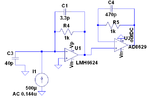
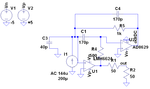
I'm working on a rather simple transimpedance amplifier (TIA) for a photodiode. I split the photodiode current into an AC and a DC path, since I need both outputs. For each of them I use a different amplifier and a different compensation capacitor. With the values you can see in the attached schematic schematicSpice.PNG, I get a frequency response that satisfies me. The problem comes when I measure the actual frequency response of the implemented device. As you can see in the other attachment transferFunction_MeasVSsim.png 
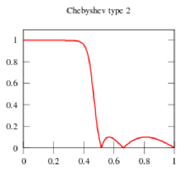
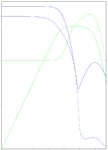
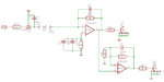
there is a strange behavior somewhere between 30 and 40 MHz in the AC channel and I have no idea what could produce it... I'm not really worried with the peaks in both channels at really high frequencies (100 MHz - 200 MHz) cause it's out of the range I need...

Some ideas about what could be happening here? Some unwanted interaction between both channels?

Thank you so much in advance.

Best Regards.
 

The parallel structure looks strange and isn't well considered, I think. Even if the low frequency path won't disturb the high frequency transmission, it will at least add noise. And it probably does more.

If you look at the AD8629 output impedance characteristic, you get an idea how it can affect the high frequency behaviour. The OP models aren't very exact, apparently.

Figure out a different topology, at least keep the low frequency path from shorting the RF signal.
 
Thank you so much for your quick reply.

I have in mind two possible alternatives, the addition of a common first stage using the same OpAmp as in the AC path (LMH6624) or the addition of some passive components in the DC part to isolate it from the AC. If you went for the second one, what would you think it's better... RC low pass filter or a combination of inductors and capacitors?

- - - Updated - - -

Thanks to your suggestion, I realised there is a peak in the output impedance of the AD8629 at 30 MHz approx... too much for a coincidence. But I don't really see how this peak in the output impedance could affect the output of the other opamp... decreasing its gain...
 
Last edited:

Counterquestion, why are you using a hybrid topology? If input current or DC gain is the reason, the "first stage" solution won't help. Instead of a parallel circuit with diplexer, you should also consider a feedforward structure where the DC path overrides the AC path at low frequencies.
 
I'm not sure if I understood it completely. By feedforward structure you mean Opamp - Opamp in series, like in the schematic I attach? (I would need to add a resistor to ground for the non-inverting amplifier) If so, then I wouldn't know how to output the signal from the first stage (AC channel) using a 50 ohms resistance for impedance matching (this resistor will change the high input impedance of the later stage, won't it?).

And about my doubt of the peak in the output impedance of the AD opamp affecting the AC channel I posted before... could it be possible to comment it a bit further?

Vielen Dank im Voraus ;)
 

Attachments

  • forwardOverride.png
    forwardOverride.png
    12.2 KB · Views: 78

Frilance, do you intentionally use single supply for the AD8629 ?
 

@LvW I use a single supply cause this specific OpAmp requires that. I chose it because it has low drift at DC and also a relatively high GBWP, and that's exactly what I was looking for. I used the negative supply since I will get negative voltages when the current flows through the photodiode.

@BradtheRad: It does resemble a Chebyshev indeed. Maybe the peak in the output impedance that FvM pointed out creates a kind of High order low pass in combination with the compesation capacitors.

I still don't get the feedforward topology thing completely...

Thanks for your help guys!
 

Mmmm I think I get it more or less. I implemented the design in spice and I got the simulated freq response you can see attached. It actually looks quite ok, but I wanted to post here the schematic before I start thinking about implementing it on a PCB. I'm still not completely sure about how the resistors affect the gain of each part.
 

Attachments

  • forwardSimulation.png
    forwardSimulation.png
    10.9 KB · Views: 63
  • forwardSchematic.png
    forwardSchematic.png
    18 KB · Views: 75

My idea was to use the structure the other way around. The high frequency OP in inverting configuration, driving the output and feedback network, and the low frequency OP as a low-offset, low bias current input stage.

But there are many possible configurations.
 
But in that way, the output of the AD8629 can't be used to measure DC values, because the OpAmp is bypassed by the capacitor and the output is virtually connected to ground (due to the other OpAmp)
 

@LvW I use a single supply cause this specific OpAmp requires that.

Requires? Do you think that double supply is not possible?
Don´t you need a specific bias for single supply operation?
 

I agree with FvM, all it takes is <100nH with 470pF load on DC side to create a parallel high impedance resonance on the input and notch on the transfer response. Close proximity and low ESL cables are essential.
 

Requires? Do you think that double supply is not possible?
Don´t you need a specific bias for single supply operation?

I think double supply is not possible for this specific OpAmp https://www.analog.com/static/imported-files/data_sheets/AD8628_8629_8630.pdf. I chose it due to its low drift and low supply current, without noticing it's a single-supply opamp. I'm still not sure if applying a negative single power supply (-5V) affects the performance of the device (I couldn't find any information in the datasheet of this model or similar ones), but that's what is required due to the current configuration of the photodiode (it produces negative voltage at the output)


I agree with FvM, all it takes is <100nH with 470pF load on DC side to create a parallel high impedance resonance on the input and notch on the transfer response. Close proximity and low ESL cables are essential.

Mmmm could you explain where these values come from? And the concept of high impedance in parallel creating a notch is not clear to me. High impedance in parallel should help the signal flow only through the other path, shouldn't it?

- - - Updated - - -

My idea was to use the structure the other way around. The high frequency OP in inverting configuration, driving the output and feedback network, and the low frequency OP as a low-offset, low bias current input stage.

But there are many possible configurations.

Could you also comment a bit why you suggested using the positive feedback in the input stage. I thought I could figure it out myself but I'm having a hard time with that. Normally we use negative feedback since positive one leads to oscillations, right?
 

Could you also comment a bit why you suggested using the positive feedback in the input stage. I thought I could figure it out myself but I'm having a hard time with that. Normally we use negative feedback since positive one leads to oscillations, right?
It's not intended as positive feedback, gains and RC values would be adjusted so that positive feedback isn't dominant.

The basic idea of the circuit is to have overall negative feedback in the full frequency range to avoid transition edffects in the frequency characteristic. But I'm not even sure if it's required in your application. Otherwise take it as a circuit idea when playing around with amplifier topologies.
 
Mmmm could you explain where these values come from? And the concept of high impedance in parallel creating a notch is not clear to me. High impedance in parallel should help the signal flow only through the other path, shouldn't it?

- - -Response - - -

When verification shows resonance, I imagine (Series or parallel) and what stray values could cause this for inductance and capacitance in addition to the lumped circuit elements within in the (-) input to ground or feedback path, which has the opposite effect.

This would include the ground lead inductance on the scope and probe capacitance. Then I look up on a graphic display of resonant impedances called a RLC nomograph and find what intersection of LC or RC or RLC etc values exist at f for a ballpark value then target solutions by reducing suspect stray inductance in circuit or probe by reducing lead-length to zero.

RLC graph ( Keep for future use) I started using these for quick answers to resonators in 1975

www.testecvw.com/carl/images/ImpedanceNomograph.pdf

RLC.jpg
 
Thank you all guys for your feedback. I finally decided that, for this specific application, it could be easier to use the opamp in series. First I use the fast device and get a DC-coupled output that is basically flat until 80 MHz approx. Then I use the second low-drift slower OpAmp to basically monitor/slightly-amplify the previous signal and it works fine up to 1 MHz.

The problem with this topology is that I can't set 2 different gains for these 2 outputs. But I will think about a different approach in the future.

There is just one thing that seems strange. The freq response of the main output (after the first OpAmp) has a bump (I'd not call it a notch) at 1 MHz, but then it continues almost flat until 80 MHz (except for the resonance peak I control with the feedback capacitor). Suspiciously it happens more or less when the second output has its cut-off frequency...

I think it won't be a problem, but I'm just curious about what could it be.

Again, thanks to all for your answers!
 

Attachments

  • seriesAmplifier.png
    seriesAmplifier.png
    13.1 KB · Views: 80

How about this topology:
DC-Servo.png

It's a lowpass filter with a DC-Servo in its positive feedback path. This way you get a bandpass filter at the output of the LMH6624 and a separate Lowpass at the Servo-Output without the need to tap into the Photodiode connection more than once. I just replaced the AD8629 with a faster one to get a better overall frequency response. Maybe you have to select another Opamp to suit your needs.
 

Doesn't his topology have the same problem as mine, that you can't set the gain for the AC and the DC path independently?

The gain of LF path depends on the Rf used in the LMH6624.
 

Status
Not open for further replies.

Similar threads

Part and Inventory Search

Welcome to EDABoard.com

Sponsor

Back
Top