Continue to Site

Welcome to EDAboard.com

Welcome to our site! EDAboard.com is an international Electronics Discussion Forum focused on EDA software, circuits, schematics, books, theory, papers, asic, pld, 8051, DSP, Network, RF, Analog Design, PCB, Service Manuals... and a whole lot more! To participate you need to register. Registration is free. Click here to register now.

3.3 V to 1.8V level converter

Status
Not open for further replies.

erece

Junior Member level 3
Joined
Mar 17, 2011
Messages
28
Helped
0
Reputation
0
Reaction score
0
Trophy points
1,281
Activity points
1,470
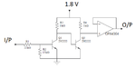
I want to convert a square wave with high level of 3.3 V & low level of 0V to a square wave of high level of 1.8 V and low level 0V. Frequency of square wave is 1 MHz in one case and 25 MHz in other case. I have the circuit for the converter as shown in the figure. I simulated this circuit both in LT Spice & Tina. The circuit simulation is working for 1MHz signal but with some delay. And it is not working for 25 MHz. May be because switching time of BJT is high as compared to period of the signal. Suggest some alternative for that or any modification in the circuit. And also I am reluctant to use any SMD level translator IC.
 

Attachments

  • Untitled.png
    Untitled.png
    11.3 KB · Views: 124

Hi,

use a single gate logic IC.

Look for VCC = 1.8V and the same time input tolerant to 3.3V.

Simple sot23-5 device or similar. Easy to use. good availability, cheap.

Klaus
 

Any time you specify voltage, high speed and logic, one also needs to specify impedance of source, load , capacitance and current.

The fanout requirements for 1 gate load are trivial compared to level translator for a clock driver with 20 loads.

The slew rate of your Op Amp is probably the limiting factor in your design.

CMOS is a much better approach to the design because the speed, source impedance and current drive is more efficient, faster and more symmetrical.

ARM uses 25 Ohm source drivers, others range up 50 to 75 Ohms ballpark and are supply voltage dependant. The impedance is derived from specs for Vol,Vol at rated current.

(Vcc-Voh)/Ioh and Vol/Iol for ESR.

But more important in logic translators is the concept of threshold and noise margin. For HC logic it is always Vcc/2 but for backward compatibility with TLL it is 1.3V threshold, so the valid logic is 0.8 for max Vol and and 2.0V Min Voh, thus it doesn't matter if it is 1.5 or 3V if it allows or is protected from over voltage.

That was just for generalization in understanding the rules for a logic translator.

Possible solution
============
CMOS logic thresholds vary with each family but designed for best noise immunity and compatibility with other logic families.
Logic levels.jpg

Without knowing your receiver, loading and noise requirements, a solution cannot be stated simply but you can specify this or learn the more generalized design approach.

**broken link removed** which types are not tolerant to overvoltage, which which types are tolerant on logic level translators. (Also includes
 

Status
Not open for further replies.

Part and Inventory Search

Welcome to EDABoard.com

Sponsor

Back
Top