Continue to Site

Welcome to EDAboard.com

Welcome to our site! EDAboard.com is an international Electronics Discussion Forum focused on EDA software, circuits, schematics, books, theory, papers, asic, pld, 8051, DSP, Network, RF, Analog Design, PCB, Service Manuals... and a whole lot more! To participate you need to register. Registration is free. Click here to register now.

internal plane problem in altium

Status
Not open for further replies.

Kick

Full Member level 6
Joined
Sep 27, 2010
Messages
344
Helped
16
Reputation
32
Reaction score
15
Trophy points
1,298
Location
India,Bangalore
Activity points
3,170
hii all,
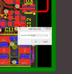
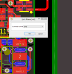
I am facing a problem in altium designer internal plane. In my design bottom side of antenna is free from copper(top&bottom) even internal plane(GND&PWR) also connected to no net. This antenna part is separated from other part of the circuit by a thick line in both GND and PWR plane,other part of the circuit is connected to GND&PWR. Problem is when I close and reopen the design,again the antenna part will connect to GND and PWR net.What should I do to get rid off this problem??

thanks.
 

VIPu,
give the thick line a net name, and it will not connect then.
keyur
 

already I did that,but after reopen the design it will again connect to net.
 

send your design ( only pcb ) and I will have a quick look. not sure what exactly you are looking for. or try to explain in deep
 

before closing the design it is free from net (GND and PWR),here I showed only GND plane.

after save,close and reopen means it will be connected to plane.
 

Attachments

  • a.png
    a.png
    48.4 KB · Views: 125
  • b.png
    b.png
    52.2 KB · Views: 122

The idea of plane is you have only one net in that layer. The idea of split plane is you can split that plane into few different net planes. when you create a split plane you must define the net of new created plane. on your screen shot it says it has no net. Try using any other net and then see the difference.
hope you understand.
thanks,
keyur
 

actually I don't want any net in that area because that is BLE antenna region.
 

you cannot leave it as a no net and define a split layer. Create a false net in schmatics ( only a wire ) bring the net in the pcb. then use that net in the new split layer and then save it and it will not combine it.
The only reason they are joining is because u r not defining a net for a split plane.
keyur
 

Status
Not open for further replies.

Part and Inventory Search

Welcome to EDABoard.com

Sponsor

Back
Top