Continue to Site

Welcome to EDAboard.com

Welcome to our site! EDAboard.com is an international Electronics Discussion Forum focused on EDA software, circuits, schematics, books, theory, papers, asic, pld, 8051, DSP, Network, RF, Analog Design, PCB, Service Manuals... and a whole lot more! To participate you need to register. Registration is free. Click here to register now.

Negative Inductor Current of Boost Converter

Status
Not open for further replies.

BKI

Member level 1
Joined
Jul 23, 2014
Messages
33
Helped
0
Reputation
0
Reaction score
0
Trophy points
6
Activity points
264
Hi,

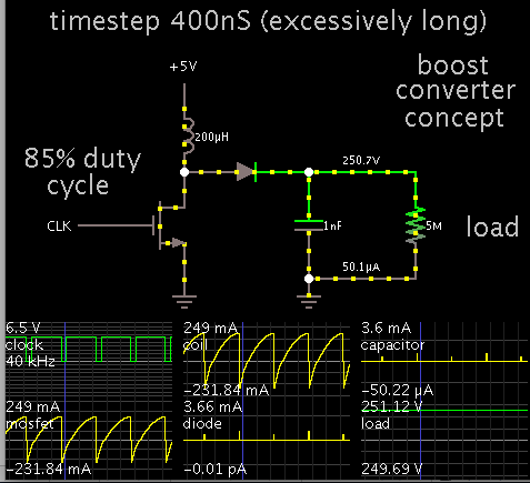
i have designed a Boost Converter that generates 250V from 5V supply. It operates in DCM, has a high impedance output (5Mohm) and low output current (50uA).
The MOSFET has a input signal with a frequency of 40kHz and Duty Cycle of 0.9. In the Cadence simulation, the circuit works well, but the inductor current looks strange.
When the MOSFET is switched off, the inductor current falls in negative current range. So, the inductor peak current is around 740mA and the minimum inductor current is around -40mA. I am using a external real diode model from Vishay (byg20j) for Cadence simulation.

What can be the reason for the negative inductor current?
I am not sure if i have to worry about it!

Thanks in advance for your help!
 

Hi,

usually the current does not change direction in an inductor (but voltage does)

So please post your schematic and a scope diagram (with magnitudes of timebase, voltage, current).

Klaus
 

I have attached the schematic and signal diagram. Hope this helps to find solution screenprint.jpg.pngZeichnung Boost Converter.jpg.png.


Hi,

usually the current does not change direction in an inductor (but voltage does)

So please post your schematic and a scope diagram (with magnitudes of timebase, voltage, current).

Klaus
 

Hi,

is it really negative? please zoom in.
I see it is very near to zero.

From my understanding it should be >=0.


Klaus
 

Believe me, its -40mA. And this already has an effect on the power efficiency. So, i want to avoid this. But mostly i want to find out what is the reason.
In the meantime, i found out that the current is coming from the MOSFET. But i don´t understand why.
 

When the switch turns off, the center node jumps to 250V for an instant.

Of course we realize the inductor is generating this high volt level.

However I believe the simulator algorithm 'forgets', and treats the node as a source of the 250V.

It makes a convergent solution difficult. But the simulator must find one. So it handles the situation by creating a small reverse current flow through the coil, at least for a frame or two.

You may find the reverse current is different when you try different timesteps.
 

Do you have any suggestions, how can i find out if the problem is simulator based?

When the switch turns off, the center node jumps to 250V for an instant.

Of course we realize the inductor is generating this high volt level.

However I believe the simulator algorithm 'forgets', and treats the node as a source of the 250V.

It makes a convergent solution difficult. But the simulator must find one. So it handles the situation by creating a small reverse current flow through the coil, at least for a frame or two.

You may find the reverse current is different when you try different timesteps.
 

The simulation waveforms don't show much details.

But generally it's expectable that the drain voltage swings below ground due to transistor and diode capacitances. If you observe the simulation results thoroughly, you should see why and how.

You shouldn't particularly worry about the negative currrent. The exponential current waveform suggests however a low converter efficiency.
 

Do you have any ideal how i can make the current waveform more linear than exponential.
I am not sure if this is caused by the load and not avoidable.
I thought about using Power regulation to increase the efficiency, but i am not sure if this really solves the problem.
Or is the exponential trend probably caused by the fact, that i used an ideal inductor ?

The simulation waveforms don't show much details.

But generally it's expectable that the drain voltage swings below ground due to transistor and diode capacitances. If you observe the simulation results thoroughly, you should see why and how.

You shouldn't particularly worry about the negative currrent. The exponential current waveform suggests however a low converter efficiency.
 
Last edited:

The exponential waveform is caused by the inductor (and possibly MOSFET) series resistance, respectively a too high inductor current. In other words an unsuitable circuit dimensioning.

It should be considered that 50:1 boost ratio will involve low efficiency in any case. An ideal boost converter in would work with 0.98 duty cycle minimum, everything below this number is only compensating circuit losses.

It's meaningful to look at the exact current and voltage waveforms during boost phase to understand the nature of losses. The rectifier diode is seriously oversized, this may be also the case for the MOSFET.
 

Here is a simulation (in a different program) which demonstrates the same improper reverse current flow.

I got it by setting the timestep too long.

There is no way it would happen in a real circuit.

6232536900_1406220213.png


By shortening the timestep, the reverse current becomes less.

Also notice the positive part of the waveform is not linear. It is starting to level off. This is caused by the mosfet not fully turning on. This limits current flow. It can also happen if there is internal resistance in the supply, or the coil.
 

Hi,

Regardeing the negative current in the coil.

It might be because of reverse recovery effects.
After switching off the fet a high voltage is charging the output capacitor. But as soon as the inducor is "empty" the voltage drops. Now the capacitor is at much higher voltage than the supply. But the diode is still conductive. It needs a smal time for the diode to become high ohmic. This effect may cause the reverse current.

--> Try to find special high speed switching diodes and simulate again.

This also meets your statement, that the reverse current decreases efficincy, because it discharges the output capacitor a little.

Good luck

Klaus
 
I agree that diode reverse recovery time can cause the discussed negative inductor current, but as far as I see, even with ideal diodes the unavoidable transistor output capacitance will do the same. In so far it's just normal circuit operation.

As already stated, I don't think that the negative current is a dominant circuit problem.

The diode is already an "ultrafast" type, but unreasonably oversized.
 

Thank you very much for all your help! I think the negative current reason is clear now.

But it would be nice if some of you have suggestions regarding the exponential current flow.
Any way how to get it more linear? Or is this also unavoidable?


Thank you very much!
 

Hi,

Any way how to get it more linear?

The less DC resistance, the more linear and the lower the power loss.
And maybe it´s caused by the ON resistance of the FET.

From what i see the DC resitance of the FET added with the dc resistance of the inductance may be in the magnitude of 4-5 Ohms.

I´d say 0.3 Ohms or lower should give an acceptable efficiency.

**********
The duty cycle of 98% that FvM mentioned is for full load with your given data.
I reccomend to build an overvoltage protection circuit in case of less or no load current.
This overvoltage circuit may switch off clock until voltage dropped (burst mode = low power) or continously lower the duty cycle down to 0% (continous mode = low voltage ripple).

Klaus
 

Status
Not open for further replies.

Similar threads

Part and Inventory Search

Welcome to EDABoard.com

Sponsor

Back
Top