Continue to Site

Welcome to EDAboard.com

Welcome to our site! EDAboard.com is an international Electronics Discussion Forum focused on EDA software, circuits, schematics, books, theory, papers, asic, pld, 8051, DSP, Network, RF, Analog Design, PCB, Service Manuals... and a whole lot more! To participate you need to register. Registration is free. Click here to register now.

[SOLVED] Power supply current source/sink capabilities?

Status
Not open for further replies.

David_

Advanced Member level 2
Joined
Dec 6, 2013
Messages
573
Helped
8
Reputation
16
Reaction score
8
Trophy points
1,308
Location
Sweden
Activity points
12,219
Hi,
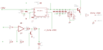
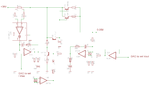
I'm building a power supply based on a voltage regulator(TPS7A4701) but as I search for information about if my design is worth paying to build I find people saying something about that problems might arise when pulling the regulator output down to zero if it need to sink some current from the load to do so.

What kind of power supply can sink source and sink current?
 

Hi,

First check the datasheet, there usually is all the information you need.
Usually there is a typical circuit you can refer to.

What exactely is the problem?

A power SUPPLY usually can source current, and the load can sink current.

pulling the regulator output down to zero
Pulling the VOLTAGE down to zero generally is no good idea, because the job of the regulator is to regulate a constant output voltage.
Pulling down the output to any other voltage will end in current overload.

In the datasheet you will find the maximum current you may draw from the output, but the voltage stays the same...

Please give us the values ( input voltage, output voltage, min. load, max load....) that you expect and we can give you better answer.

Klaus
 
  • Like
Reactions: David_

    David_

    Points: 2
    Helpful Answer Positive Rating
what exactly you want i didn't understand. Few loads connected to Regulators will both source and sink. When we are connecting that kind of load to power supply, regulator should be capable of sinking current.

for ex: DDR2/3 VTT termination regulator needs to both sink and source
like LTC3618,TPS51116, MAX17000 etc....
 

A supply that both sources and sinks current is essentially a big power op-amp.
Several companies make them, including STMicro, Linear tech which offer ICs that go over 1 amp at 30 volts.

If you require higher power, you will have to go to modular power opamps, like these:

**broken link removed**
 
  • Like
Reactions: David_

    David_

    Points: 2
    Helpful Answer Positive Rating
Well there is something that I don't understand but this is a design that I'm considering building, for one thing it would not be a common thing for me to force it to output 0V but the circuit would be able to do it. That NPN darlington connected to the regulator output is a recent addition and one that I have to read more about, I read and I read but there is some stuff with transistors that I do not get.

A big problem is that my living situation keeps me from using my equipment to experiment, I would have taken a LM317 with its output connected to the base of some NPN transistor and observe what would happen but I can't get at my things for a while. After finding out how a regulator acts when forced to 0V.
the schematic leaves out some things like digital control of the Set/Adj voltage, but the purpose of this power supply project is for me to learn software and circuit board layout, as well as anything els I guess. I am in the progress of writing the software but then I find my self really questioning if I really should enable it to force the output to zero volts, beside learning I want to produce as good of a power supply as I can.

As I can't test things out for now I am kind of in the blind and some of the parts cost more then I want to throw at my blind guess, simulation gives me no results, I don't know why but the program I use breaks down for some unknown reason.
I am sure most of the project will work but the output voltage down to 0V is something I clearly don't understand, but does a output "stage" with some arrangement of transistors change things?

One important thing is also that I do need a good power supply to be able to experiment with other things, so at some point learning is not going to advance before I can use a adjustable power supply to test things out for my self.

- - - Updated - - -

I have not had any official education and I am teaching my self, that leaves some gaps though and I find my self having need for things I don't quite know how to ask for.
 

Attachments

  • eda.png
    eda.png
    12.1 KB · Views: 225

Hi,

Read the datasheet carefully, especially section "Adjustable operation"

1) the most importent thing to change is:
connect FB to center tap of a voltage divider to your OUTPUT voltage (emitter of T12)
This is the meaning of this pin. It is not meant as an input to change output voltage (although possible).
The voltage on this pin is ALWAYS 1.4V +/- 0.5%. Otherwise it is out of regulation.

2) In your circuit the 5 x 10uF must be connected to the output = emitter of T12, not output of TPS...

3) The MJ3001 is to get more output current.
What max. output current do you need?
Mind: This transitor decreases max ouput voltage, because it increases voltage drop to max. 1.5V.

4) Use a 100 Ohms resistor between E and B of T12.

5) use a small capacitor between pins 1*2 and pin3 of TPS..

6) instead of LM334 use a 10k resistor to GND

7) check if "+" of C13 is properly connected ( there is no visible junction)

If you want to setup your output voltage why don´t you use TPS7A4700? With it you can "digitally" setup output voltage in steps of 0.1V.

please dothis changes first then show the new schematic.

*****
To go on:
If you want to use TPS7A4701 in future:
* What output voltage range do you need?
* How do you want to adjust utput voltage? pot, digital pot, ucontroller, filtered PWM, DAC...
* I recommend to use a current limit circuit to protect from overload/overheat/destroy

Klaus
 
  • Like
Reactions: David_

    David_

    Points: 2
    Helpful Answer Positive Rating
I am making the changes to the schematic but first,

1, I have been getting ideas from other projects that use LM317 or LT3081 as regulators that are being supplied a external voltage to its adj/set pin, if that is not viable here then I have to change regulator.

2, done.

3, max current will be 2,5A, an increase in drop out voltage is not a problem. I have 35V at the input and want to be able to get 30V out.

4, done.

5, see below.

6, done, I'm looking for options fort driving a LED from the output but the voltage range possible at the output makes it difficult.

7, done.


I'm not sure how I deduced that this was a viable circuit, but from the get-go I had planed to use LM338 and feed a voltage to the Adj pin to set the output voltage. I have forgotten about checking that this regulator can work in the same manner, the idea is to use a 16-bit DAC to set the output voltage in the range 0V(or perhaps 1,4V) to 30V. If I would go for 0V capability then I will need to add a "inverting charge pump" that will be driven by a 32kHz PWM signal from a MCU to get a -3V supply rail.

It might not be its intended use to supply a LM317 adj pin with a external voltage but it works, might it be a viable way of controlling this to?
The main thing that attracted me to TPS7A4701 is that it is adjustable from +1,4V to 34V and have a enable function but LT3081 might be a replacement in this circuit, its datasheet clearly says that the regulator can be adjusted with a external voltage supplied to the set pin.

I have a LT6105 measuring current and outputting a voltage proportional to the current through its sense resistor. That voltage is buffered by two unity-gain op-ams, one buffers the voltage to a ADC and the other buffers the voltage to be compared with a comparator with a voltage created with a DAC. I have not compleated the comparator circuit, stumbled on some trouble understanding LM311 and how to control the output voltage but one way or another the idea will be implemented.

I want a way to set the regulator output voltage with a variable voltage produced with a DAC, I have found a design(two actually) that is based on discrete transistors, load regulation is better and thermal stability is mostly dependent on two resistors. One of them just happen to use LT6105 as well, the second schematic is just a re-draw of a design by Kerry D. Wong but I'm leaning of changing the design, now that I have put all this time into the regulator design it seems more and more as a discrete solution is more suitable
But I can't tell which approach will produce the better power supply, if I go with op-amps/transistors I have to watch out for oscillations but I would learn more. One thing that concerns me is that the regulator design seams to have significant lower output noise, and that is a important parameter for me.

There will be two identical isolated voltage rails and one isolated MCU control circuit with one 182x64 LCD display, Two encoders, one for each channel and one keypad. As well as different buttons to enable the channels and connect them in different arrangements etc.
 

Attachments

  • new.png
    new.png
    42.4 KB · Views: 139
  • kerry.png
    kerry.png
    17.5 KB · Views: 140
Last edited:

Hi,

Yes, as Borber mentioned there is no true sink capability in this circuit.
Do you need it? If yes, how much current and how fast?

Voltage adjust. It is possible to " manipulate" output voltage with the adj pin. But it ALWAYS needs the feedback from the output.
The manipulation is done by feeding CURRENT to the node and not by feeding a VOLTAGE to the node as in the first circuit. Voltage always is about 1.4V at this pin. Check other circuits on this.

To 5) For stability reasons the capacitor C32 must be connected to the output 1*2.

You don't need the negative supply to go to 0V. Indeed you need a resistor fom a positive voltage to the adj pin to manipulate for lower output voltages.

In general there is no need to change to an other regulator. All can be done with this device.

Current measurement/limit:
The use of the two unity gain buffers is not wrong, but there is no need for them.
current ADC measurement is ok.
Current limit with a comparator here is no good idea because it is a "switching" limiter. During overcurrent condition you will see the regulator output to oscillate. Not nice. Try to find a smooth regulated current limit.

Voltage setting:
The DAC, one Opamp and some passive parts will do the job ... with the TPS regulator.
(Btw. In you discrete circuit Q6 must be an NPN)
In your schematic R26 and R27 adjust the output voltage. From the datasheet you know that the voltage must be 1.40V and the current to Gnd is about 350nA. As R27 the value of 10k is recommended.
With 1.4V and 10k it gives 140uA through R27. Add the 350nA and now you know the current into this node. 140.35uA.
If you now want an output voltage of 30V then there is a voltage of 30.0V - 1.4V = 28.6V across R27.
R27 = 28.6V / 140.35uA = 203.776 Ohms.Take 200 kohms
This was the fix setting of output voltage.
Now with variable output voltage. The challenge is to manipulate the adj node curents.
I now try to use an opamp with single supply of 5V. I decide a max useful output voltage of 4.5V.
If a current flows from 4.5V to the adj pin means that through R27 needs to be less current. Thus lowering the output voltage.
For R27 = 156k and R_DAC = 20k81 you get 30V down to 0 V with 0.5 upto 4.5V .

With the ucontroller it should be no problem to to calibrate to 0V and 30.0V.

Hope this helps.

Klaus
 
  • Like
Reactions: David_

    David_

    Points: 2
    Helpful Answer Positive Rating
schmit trigger in his post #4 explained the concept of power supply which can source current to the load or sink it from the load. Single transistor on output can only source current or sink it and not both.
 

The sink/source question arose by me reading that a power supply might need to sink some current from the load in order to bring the voltage down to 0V, but I've gotten the answer about sink/source by now.

Thank you very much Klaus, it will sure help allot.
I have gone through the datasheet in detail but I could not deduce what you have provided me with, but you've sent me back on track.
It will take some time to draw it up to understand but I will post a update here when I have implemented your guidelines, this is just great:)

Thank you all.

- - - Updated - - -

By the way, I don't even no what type of load would require source and sink capable power supply.
This design will be used as a general purpose power lab power supply but I followed up on the tip from schmit trigger and found some interesting high current op-amps, but regarding sink/source, if one would make a dual power supply with LM317/LM377 then the positive rail would source current end the negative rail sink current. Is sink/source always tied to negative/positive voltage?
Or can a positive supply voltage sink current?

- - - Updated - - -

I think I got it, sink: draw current away from, source: supply current to. Regardless of voltage polarity?
 
Last edited:

Hi,

sink/source:

In my eyes usually (not generally) power supplies are only specified to source current.

Look at it from the "power" side. The supply is the source of power, the load is the sink of power.
The same is for dual power supplies (one for the positive voltage, one for the negative voltage)

As mentioned before the disadvantage of a "source only" power supply is when there is a big capacitor charged with 20V for example and you tell the supply to output 5V. Then the supply is not able to discharge the capacitor, so it takes a long time until voltage drops down to 5V.
For sure there are possibilities to implement this in TPS.. design. Just use a comparator comparing the ADJ voltage with 1.45V (a bit more than the nominal 1.4V). If ADJ is too high then enable a simple constant current source to discharge the output with constant 100mA or similar.

But if you have a true positive negative supply where you have an output range of +/- 30V at the same two connections, then i t acts like a big OPAMP id therefore it must have sink and source capabilities.


If i want to build such a thing, then i´d look for
* DC coupled class D audio amplifiers (BTL also possible).
* or full bridge
* or halfbridge power stages.

The advantage of the ClassD audio is that they usually have built in protection (overcurrent, overheating...) and are optimized for low noise (hopefully).

Klaus

edit: generally --> usually
 
  • Like
Reactions: David_

    David_

    Points: 2
    Helpful Answer Positive Rating
It's very unusual to require a power supply to both sink and source current. Only if you have a specific load in mind that needs to both sink and source current should you bother with designing a power supply that would do both. It significantly increases it's complexity.
 
  • Like
Reactions: David_

    David_

    Points: 2
    Helpful Answer Positive Rating
I have gotten the answer sought after in the thread title but the tips and help from Klaus is somewhat related, I have spent many hours simulating the proposed circuit arrangement but its been problematic to say the least.
For one I haven't found a good representation of the regulator in question, I have been using Multisim from National Instruments and they have some voltage regulators available but they all react differently to my circuit.

The values in the schematic is just something close to what Klaus posted, but I begun trying to deduce what changing values would do but in the end I just put pots in instead but no matter what values I use the range of adjustable output voltage is limited to ~ 4,5V and the lowest I can get is some mVolts above the reference voltage of whatever regulator I use. The more I experimented with different values as well as a couple of different op-amp arrangements the more confused I got and I don't really trust the simulator, sometimes the results almost flashes with a banner saying "Does not compute".
During all my involvement with electronics I have always been focused on voltage, I've looked at Thevenin theorem but not Norton but I will have to learn more about the current side of things.
But for now I'm stumped, ant thoughts?
I'm obviously making some mistake/mistakes.
 

Attachments

  • lm317.png
    lm317.png
    4.3 KB · Views: 136

Hi,

You can do it with almost any voltage regulator.
With your circuit.
Use 156k for R1,
10k for R2
And 20k8 for R3.

Because the new regulator has other adj voltage you may see other output offset.
Adjust R2 to get the right offset.

Because 156k / 20k8 = 7.5 makes your output range 7.5 * input voltage range.
With a pot on 0V and 5V you get 7.5 * 5 = 37.5V. Theoretically, because ther are the suuply rails.

Good luck.

Klaus
 
  • Like
Reactions: David_

    David_

    Points: 2
    Helpful Answer Positive Rating
To be honest I don't understand how you found all the values, in the datasheet I can only find that a minimum of 5µA needs to run from the output to ground, but I will figure it out in the end I'm sure.
The values where spot on though, I am sure I've already tried the circuit that I currently have running, but this time it works. The differences regarding which regulator respond the way we want in this situation as far as I can tell is if the voltage at the Adj/Sense pin is referenced to the output or to ground, the ones that have a Adj voltage referenced to ground is the ones that suit this application. And those are the ones that have a separate ground terminal as well, makes sense.

When the op-amps output voltage is below the regulators Vref is the op-amp sinking current?
I will be using a quite expensive DAC and it can source and sink way more current than is needed here,
I would not bother any one with this question if it wouldn't be that I simply can't economically afford a screw-up, is there any danger in using the DAC output directly?

I am much happier with this approach but I have read and searched the internet excessively for circuits to control adjustable regulators and this one never shows, since you gave me this hole thing I want to ask if you mind me(when I have a complete set-up and grasp of it) would write a how-to or something about this approach to spread around?

Thanks for all the help, my final design will be so very much simpler now.

- - - Updated - - -

I will start a new thread to further discuss this circuit is there are interest in that.
 

Hi,

When the op-amps output voltage is below the regulators Vref is the op-amp sinking current?
True.

I will be using a quite expensive DAC
Why? Use the dac you have, it just needs a voltage output (no current output)

The current in/out of the dac is low, usually no buffer is needed.

ask if you mind me
I don't mind... maybe we can discuss it before...

Klaus
 
  • Like
Reactions: David_

    David_

    Points: 2
    Helpful Answer Positive Rating
I have learned a lot since I settled on DAC8574, I guess when it comes to 16bit DACs it is not that pricy compared to what one can pay but 19USD is still ALOT.
But after the changes brought on here I can get away much cheaper, especially since I have come to understand that in a closed-loop application INL is not that important. DAC8574 is a really nice quad DAC, before I needed 3 channels and thought to prioritize all specs, now I need 2 channels and know that I can loosen up on the specs, I think it will be 2 single 16bit DACs for each channel. One for voltage setting and one for current setting, even with external reference for them it will be cheaper(if not free) but I am still looking for the most suitable option. It is all I^2C so multiple chips hardly increase the complexity at all, I am going to add some hysteresis to the current control comparator and then(if that works out) the hardware should be pretty much done.

Having a working example of the circuit really helped in understanding the values, It will be quite a while before I can set time aside to write anything but I promise I will get back to you about it before I post anything anywhere.

Your help has really been invaluable, a thousand thanks.
 

Status
Not open for further replies.

Similar threads

Part and Inventory Search

Welcome to EDABoard.com

Sponsor

Back
Top