Continue to Site

Welcome to EDAboard.com

Welcome to our site! EDAboard.com is an international Electronics Discussion Forum focused on EDA software, circuits, schematics, books, theory, papers, asic, pld, 8051, DSP, Network, RF, Analog Design, PCB, Service Manuals... and a whole lot more! To participate you need to register. Registration is free. Click here to register now.

[SOLVED] dc offset canceller circuit

Status
Not open for further replies.

matin-kh

Member level 3
Joined
Nov 9, 2013
Messages
67
Helped
0
Reputation
0
Reaction score
0
Trophy points
1,286
Location
iran
Activity points
1,955
hi every one,
This circuit is used as dc offset canceller but I can't understand how it works.
1.jpg
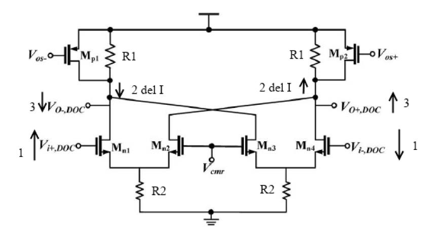
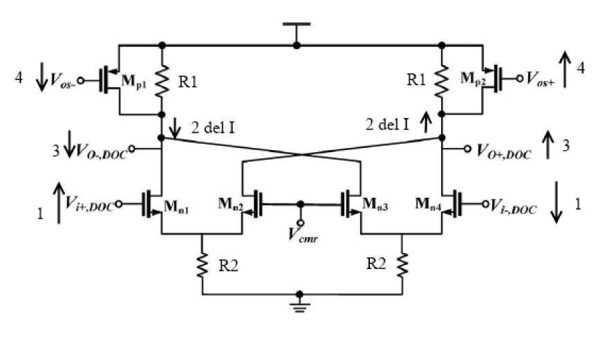
it is the block diagram of circuit which you can see DC offset canceller in it:
2.jpg

In the paper it explains as below:

"In this design, a Ft doubler scheme is proposed for inclusion to the dc offset canceller, as shown in This structure cancels the dc offset voltage and simultaneously corrects the common mode voltages of the outputs of DOC to a desirable level Vcmr . The value Vcmr is chosen at the midpoint of the calculated input common voltage range and its voltage is fixed by the resistor ratio"

I can't understand the duty od Mp1 Mp2 and i don't know that all the transistors are in saturation region or not. and one more question it says that the output dc voltage is equal to Vcmr how could it be possible the dc voltage of input and output be equal?
could you please tell me how this circuit works and response my questions?

best regards
matin
 

Hi there. I am having a go at this. I might be wrong though.

From your figure 1 it looks like they have assumed a positive offset in the left arm and negative offset in the right arm

Figure 1:


The numbers in the figure indicate the order in which the direction of the voltage/current varies. As you can see if we have an offset in the direction given (1), the current changes in the direction given (2) which results in change in the output voltage in the direction given (3).
After the amplifiers A1,A2 and A3 we have a feedback network (see the naming convention that I have used in the figure below)

Figure 2:


This will change the control voltages in the below figure in the direction given (4)

Figure 3:


So that the changes in del I current gets compensated and the current through the resistors R1 goes towards its original value and thereby the output voltages of amplifier A1 also go towards its orginal values. But where does it stop? It stops when the complete feedback path in figure 2 is valid. If A2 and A3 are large enough, ΔVout in figure 2 will settle at the control voltage so that ouput voltages of A1 is very small (which depends on the A2A3 gain). In order to have a very less ΔVout we should have the gain A2A3 and the offset transistor Mp1 and Mp2 (decides the offset gain) to be huge.

The RC filter in the feedback network is there for allowing only dc (offset is a dc phenomenon) and doesn't allow the signal (which is the input to the VGA and can have a very high frequency) to alter the offset control voltages. By this way we ensure that the signal doesn't affect the offset control voltages.

The common mode is chosen in the midpoint of the input common mode range so that you get maximum swing on either sides. The output common mode range is decided by the input common mode and the ratio of two resistors R1 and R2. Let's say there was no offset cancellation network. The current through R1 is

\[
I_{R2}=\frac{V_{cm_{input}}-V{gs_{n1,n2}}}{R2}
\]

\[
V_{cm_{output}}=I_{R2}R1=(V_{cm_{input}}-V{gs_{n1,n2}})\frac{R1}{R2}
\]

Can you just mention the paper title if possible?
 
Last edited:
thank you very much for your best description.

- - - Updated - - -

yes off course "A 5-Gb/s Automatic Gain Control Amplifier
With Temperature Compensation"
 

Status
Not open for further replies.

Part and Inventory Search

Welcome to EDABoard.com

Sponsor

Back
Top