Continue to Site

Welcome to EDAboard.com

Welcome to our site! EDAboard.com is an international Electronics Discussion Forum focused on EDA software, circuits, schematics, books, theory, papers, asic, pld, 8051, DSP, Network, RF, Analog Design, PCB, Service Manuals... and a whole lot more! To participate you need to register. Registration is free. Click here to register now.

Help me with PCB Design in Eagle Software

Status
Not open for further replies.

Yesh

Newbie level 3
Joined
Sep 24, 2011
Messages
4
Helped
0
Reputation
0
Reaction score
0
Trophy points
1,291
Location
Las Cruces, NM, USA
Activity points
1,332
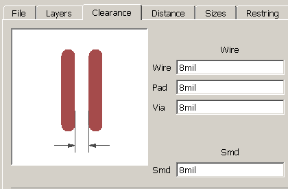
My name is Yeshwanth, a graduate student of New Mexico State University. I was working on my first pcb design as a part of Master’s Thesis. I’m using the Eagle software to design my PCB but i was getting errors when i do DRC to my entire design. The errors are clearance and width errors, these errors are popping up even i try to draw a trace width of about 8mils(which is greater than minimum width). I was wondering whether any one of you guys will be helpful in resolving my errors.

Thanks,

Sincerely,
Yeshwanth
 

Go to the clearance tool dialog and change the setting to something your PCB manufacturer will accept, maybe 6 mil?

6225401000_1403740331.png


Sometimes, a manufacturer will work with you. For example, Oshpark will accept a clearance error if it makes sense (e.g, a via in a pad that is connected to ground).

John
 

go to edit>>design rules and go to clearance tab,there you can give min. clerance value.

for width go to edit>>Net classes
 

Status
Not open for further replies.

Part and Inventory Search

Welcome to EDABoard.com

Sponsor

Back
Top