Continue to Site

Welcome to EDAboard.com

Welcome to our site! EDAboard.com is an international Electronics Discussion Forum focused on EDA software, circuits, schematics, books, theory, papers, asic, pld, 8051, DSP, Network, RF, Analog Design, PCB, Service Manuals... and a whole lot more! To participate you need to register. Registration is free. Click here to register now.

Sizing components for folded cascode amplifier

Status
Not open for further replies.

anhnha

Full Member level 6
Joined
Mar 8, 2012
Messages
322
Helped
4
Reputation
8
Reaction score
4
Trophy points
1,298
Activity points
3,684
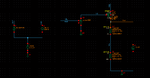
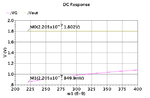
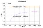
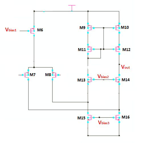
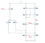
This is a folded cascode amplifier with the gain formula as follows:
Av = gm7*[gm12*rds12*rds10 || gm14*rds14*(rds16 || rds7)]
Is there a systematic way to size components so that voltage gain is as high as possible?
I am thinking about gm/Id method but how can I get load capacitance CL?
This op amp will be used for LDO but I am not sure how CL would be.

attachment.php
 

Attachments

  • Folded cascode.PNG
    Folded cascode.PNG
    37.7 KB · Views: 2,929

Hi, Anhnha;
You can choose load capacitance on the basis of UGB required for this amplifier. Just find out the effective Gm of the amplifier then Gm/Cl is your UGB. Otherwise, if you know UGB and choose Cl according to your requirement then you can calculate the Gm.
See you can increase the gain by pushing you MOS in subthreshold region where the gain is high and power is low but bandwidth reduces too much. All this thing depends on your requirement. But if you would like to maintain gain and bandwidth both then choose the value of gm/Id in moderate inversion. For large bandwidth choose strong inversion but gain reduces comparatively.
Hope you are getting me.
 
  • Like
Reactions: anhnha

    anhnha

    Points: 2
    Helpful Answer Positive Rating
Thank you.
Let's say I choose UGB = 160MHz, CL = 1pF then Gm = 160MHz*1pF = 0.16 mS
What should I do next?
 

Hi anhnha,

Taking about amplifier : In a real time scenario you will not be able to choose the load Cap CL. It will be the part of your specification.
I have a doubt regarding the gate connection of M9 and M11. M9 is fine but why has it been shorted with the gate of M11. Will you be able to keep M9 in saturation ?? I thing you will not get enough VSD for M9 ...

Talking about LDO: We don't fix the architecture before we size the Power FET in the LDO. The Power FET will give some gain of its own. So you might not need high gain from the amplifier. Again sizing the power FET will give you an idea about the output swing required from the amplifier. So a folded cascode might not be a good choice.
So take some specification of an LDO ---> Size the LDO power FET according to current required ---> Then select amplifier architecture accordingly.

Hope this helps .... :)
 
  • Like
Reactions: anhnha

    anhnha

    Points: 2
    Helpful Answer Positive Rating
Thank you, SIDDHARTHA HAZRA.

Relating to M9, you are right. I can't make it operate in saturation region. It is in subthreshold. I saw that current mirror in this patent and the article says that it is better. I used this structure for that reason.
However, I see that the gain doesn't change when I use diode connected for M9.
https://www.google.com/patents/EP0561469A2?cl=en
Could you talk in details about LDO part?
So take some specification of an LDO ---> Size the LDO power FET according to current required ---> Then select amplifier architecture accordingly.
What are the specs?
I sized the power FET with maximum W/L. I see that the large W/L of this FET is, the wider the regulated range.
For example, with W/L = 50/1, input range only 2.5 to 3 for which Vout = 1.8V
With lager W/L = 400/1, the input range now is 2 to 3 V where Vout = 1.8V.
 
Last edited:

Thank you, SIDDHARTHA HAZRA.

Relating to M9, you are right. I can't make it operate in saturation region. It is in subthreshold. I saw that current mirror in this patent and the article says that it is better. I used this structure for that reason.
...
https://www.google.com/patents/EP0561469A2?cl=en

According to the patent specification, PMOSFETs M11 & M12 have to be depletion mode MOSFETs if this circuit architecture shall work "better", s. the spec. item [0013] FIG. 13 .

Did you consider this?
 
According to the patent specification, PMOSFETs M11 & M12 have to be depletion mode MOSFETs if this circuit architecture shall work "better", s. the spec. item [0013] FIG. 13 .
Did you consider this?

I saw that current mirror in this patent and the article says that it is better. I used this structure for that reason.
However, I see that the gain doesn't change when I use diode connected for M9.
https://www.google.com/patents/EP0561469A2?cl=en

Ya if its depletion then its fine ... but as your schematic is showing MOS symbols for enhancement type, so standard architecture should work just fine.

Could you talk in details about LDO part?
What are the specs?
I sized the power FET with maximum W/L. I see that the large W/L of this FET is, the wider the regulated range.
For example, with W/L = 50/1, input range only 2.5 to 3 for which Vout = 1.8V
With lager W/L = 400/1, the input range now is 2 to 3 V where Vout = 1.8V.

Specs are the design specification that your block should meet. Say for an amplifier the target Gain / BW / Output swing / Input common mode range etc. are specifications given before designing. Depending on these requirement you will have to choose your architecture and tune it to meet them.

For LDO you will have to select one power FET size that will support the max load current specification given. There might be a case where your size supports the current but the gate voltage required is extremely low (close to VSS) then it would be difficult to keep the NMOS in the output arm of the amplifier in saturation. So while selecting a size you have to think about the gate voltage as well.
https://www.edaboard.com/threads/313153/

Once the size is fixed then note the gate voltage change when the load is changed from low load to full (or max) load.
This change in gate voltage will be the output swing specification for the amplifier. Also from the output accuracy spec. Find out how much gain is required.
Like in a buffer if you have infinite gain then the output = input. But do we actually need that high a gain (we can get infinity practically). ??
If the accuracy spec is tight then yes else 40-60dB can also serve the purpose.

As the Power FET will contribute some gain so you can budget your gain for the amplifier and choose an architecture suitably.

Hope thsi helps ... :)
 
  • Like
Reactions: anhnha

    anhnha

    Points: 2
    Helpful Answer Positive Rating
Self cascode current source works only if threshold voltage of cascode transistor is much lower (~100mV) than vth of source transistor. So M11 should be low Vt fet or has proper dimensions if only one type of devices are available. For old cmos nodes with vth roll-off for short channels, M11 should has L=Lmin and M9 L~4Lmin, while for processes with LDD/pocket/halo implants on the contrary: M9 L=Lmin and M11 L~3Lmin. In other way the M9 will be working in triode region so this source will works like single fet with L=L9+L11.

Backing to your LDO. In the last issue of Circuit and Systems Magazine is quite nice paper about CL-LDOs
 
  • Like
Reactions: anhnha

    anhnha

    Points: 2
    Helpful Answer Positive Rating
Thank you very much, everyone.

SIDDHARTHA HAZRA, I am reading the thread you gave about choosing power mos size. That is really helpful.
Could you tell me how to simulate load capacitance CL at the output of error amplifier for LDO in cadence?
I think after power FET size is fixed, CL should be fixed.
 

Hi, SIDDHARTHA HAZRA.

I just simulated the power FET as your suggestion.
Here is the picture:

Schematic for simulation:

attachment.php


0mA load current simulation:
I could find the W and L so that Vout = 1.8V. With L = 180nm, W = Wmin = 220nm => Vout = 1.802V

attachment.php


And this is 10mA load current simulation.

W/L = 122.4u/180n

attachment.php


So, the output voltage swing of error amplifier is 106.5mV to 851.22mV.
W/L of power FET is 122.4u/180n

Can I choose a bigger W/L for power FET? For example, W/L = 500u/180n. What is the problem with that?
 

Attachments

  • Power-FET simulation.png
    Power-FET simulation.png
    11.7 KB · Views: 825
  • VG-0mA.png
    VG-0mA.png
    5 KB · Views: 776
  • VG-10mA.png
    VG-10mA.png
    4.9 KB · Views: 772

Hi anhnha,

1) How to measure Power FET gate capacitance for error amplifier: You can just measure the Cgs + Csg + Cgd+ Cdg (at both load conditions) reported by the tool. Both high and low load conditions are necessary as the VSG of the MOS will change and MOS capacitance will change as it depends on the gate voltage.

2) Your current VG range is 0.106V (at full load) to 0.851V (at low load) .... considering the full load I don't think 106 mV is not a sufficient VDS for the output NMOS of the error amplifier. So you should try with a higher width this will shift the total range upwards. More over in the low load its just 0.851 V so you have enough margin on the upper side. So you should increase the Power FET size.

I hope the voltage supply is 2V so try to keep the VG mid way, as your Vg swing is around 750mV so a VG of 0.650V (at full load) and 1.4V (at low load) should just work fine. Size Power FET to get a range close to it. Then go ahead and design your amplifier.

Hope this helps .... :)
 
  • Like
Reactions: anhnha

    anhnha

    Points: 2
    Helpful Answer Positive Rating
Thank you for the detailed explanation.

Could you please look at the slide at the page 37 about how to determine size of power FET?
According to that method, my power FET should have W/L about 8775.
But according to your method, W/L is much smaller.
 

Could you please look at the slide at the page 37 about how to determine size of power FET?
According to that method, my power FET should have W/L about 8775.
But according to your method, W/L is much smaller.

Slide 37 of which doc .... can u give the link....


Ya if you want a text book solution then its fine. You assume u and Cox values and then use the current equation of a MOS in saturation and calculate the W/L.
But practical device models are way too complex as it captures the behavior in silicon (might not be 100%). A small example in Slide 37 they have assumed Vgs - Vth = Vdsat and has used it in current equation but in practice they are not equal.

The magic of characterization is that you need not depend on the MOS parameters like u and Cox. What ever it is, will automatically be taken care by the simulator. You need only observe the voltage input and current output and the W/L at which your target is achieved and look at the test bench used to characterize the Power FET. It is exactly a model of LDO. So it is more close to the actual application. So if the hand calculation gives you a W/L of 8775, then just apply it in the test bench and observe the VG value. It will be close to VDD (2V) at low load. Now as the VG is the output of the amplifier the output arm PMOS will be in linear region.

Hope this helps .... :)
 
  • Like
Reactions: anhnha

    anhnha

    Points: 2
    Helpful Answer Positive Rating
Thank you for the detailed help.
Now I need an opamp for bandgap with high gain (more than 80dB) and low power (not more than 30uW). Could you suggest a topology for that?
.
 

Regarding the gm/ID method, you may want to look into this paper: "Design Optimization of High-Speed and Low-Power Operational Transconductance Amplifier Using gm/ID Lookup Table Methodology" by Shoichi Masui and Boris Murmann. IEICE Transactions on Electronics, Vol. E94.C (2011) No. 3 P 334-345 .

But you may find that, while the gm/ID method extends the scope of the traditional pure equation-based analog sizing methods into the moderate inversion region, it is difficult to apply for low power optimization of complex real world designs. It still requires developing a detailed sizing strategy for every topology, and may need many iterations for power minimization under specification constraints with trade-offs. And then think about process corners, local variation etc. which can have a more severe effect on low power designs.

As soon as you go beyond textbook examples and do productive ultra low power design optimization, I recommend looking into fully numerical circuit optimization methods. The gm/ID method can still give a good starting point for circuit optimization software, but is not a necessary requirement. A good circuit optimizer can solve in minutes Opamps of a complexity that takes you weeks to develop and debug a gm/ID sizing strategy.
 
  • Like
Reactions: anhnha

    anhnha

    Points: 2
    Helpful Answer Positive Rating
Thank you, micpro.
I will study that paper and get back later.
 

Hi, everyone.
I am using gm/id method to design the folded cascode amplifier.
From Cload and GBW, I can determine gm of M7 and M8 => W/L of these transistors.
But how about other transistors?
How should I size them?
Also, how can I use specs DC voltage gain, Av?

105764d1401110946-folded-cascode.png
 

Status
Not open for further replies.

Similar threads

Part and Inventory Search

Welcome to EDABoard.com

Sponsor

Back
Top