sakibnaz
Full Member level 3
Hi all.
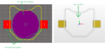
I have a Cell Coin CR2016 Battery Altium Footprint. I can see the +Ve pads are on Top Layer but the -Ve Pad is Top Solder. Now in 3D View the Top Layer Pads i.e. +Ve Pads are only visible. Top Solder i.e. -Ve Pad is not. So how the Battery -Ve terminal will get the contact? Or I need to change the -Ve Pad from Top Solder to Top Layer?
Attached is a picture for your review.
Sorry ... if ques is silly.
Regards.