Continue to Site

Welcome to EDAboard.com

Welcome to our site! EDAboard.com is an international Electronics Discussion Forum focused on EDA software, circuits, schematics, books, theory, papers, asic, pld, 8051, DSP, Network, RF, Analog Design, PCB, Service Manuals... and a whole lot more! To participate you need to register. Registration is free. Click here to register now.

Folded cascode amplifier with sub-blocks

Status
Not open for further replies.

anhnha

Full Member level 6
Joined
Mar 8, 2012
Messages
322
Helped
4
Reputation
8
Reaction score
4
Trophy points
1,298
Activity points
3,684
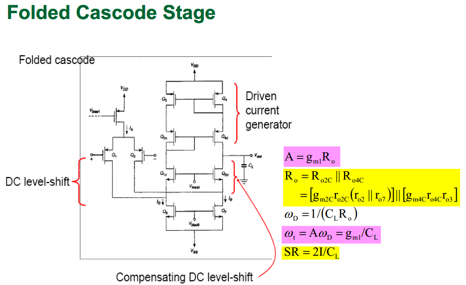
I saw this picture of folded cascode amplifier somewhere in a slide lecture. The problem is that the writer didn't give any explanation about subblocks in the picture.
As you can see, there are blocks:
- DC shift level
- Compensating DC shift level
- Driven current generator

I have searched a lot for how these blocks work but found nothing.
Could you please, explain how they work or give some links with explanations?
Thank you.

attachment.php
 

Attachments

  • Folded cascode.PNG
    Folded cascode.PNG
    90.5 KB · Views: 2,278

Hi anhnha,

The correct way to approach a folded cascode understanding is to start from a telescopic cascode amplifier and then try to visualize why folded cascode is important.
DC Shift is clear as the Drain of Q1 will be lower than the input DC level and compensating it by Q2C. But really you wont find an author naming them like that in any book. It might be just for the explanation purpose.

It will suggest the book of Razavi. This will clear most of you doubts about how a folded cascode works.

I had a doubt with the Ro equation: the second part Ro4C = gm4C * ro4c * ro3 will this be ro3 or 1/gm4 .... I might be wrong but please do a small signal analysis of a CS casode amplifier where the top MOS is diode connected as in this pic .

Hope this helps ............. :)
 
Thank you very much, SIDDHARTHA HAZRA.

I am reading up about folded cascode amplifier. Hope you will help again.
DC Shift is clear as the Drain of Q1 will be lower than the input DC level and compensating it by Q2C. But really you wont find an author naming them like that in any book. It might be just for the explanation purpose.
I see it now.
I think the DC shift level and compensating DC shift level are not really main functions of Q1, Q2 and Q1C, Q2C, right?
To me, it seems that transistors has below functions.
Q1, Q2: to amplify input signal
Q1C, Q2C: I don't know any except for compensating DC level shift.

I had a doubt with the Ro equation: the second part Ro4C = gm4C * ro4c * ro3 will this be ro3 or 1/gm4 .... I might be wrong but please do a small signal analysis of a CS casode amplifier where the top MOS is diode connected as in this pic .
I think you meant ro4 or 1/gm4 not ro3 or 1/gm4.
I think you are right.
I just calculated output impedance of cascode structure Q4 and Q4C and got Rout = ro3 + ro4 + gm4C*ro4c*ro4 which is approximate to gm4C*ro4c*ro4.
 

Hi anhnha,

1) Ya you are correct ....

2) The equation in your first post says gm4C * ro4C * ro3 ..... first of all why ro3 ..... better it should have been ro4 ..... but what I think it will be 1/gm4 as the small signal resistance seen from the drain of a diode connected MOS is 1/gm .... So shouldn't the total gain equation look like Gain = gm1 * (gm2C * ro2C * (ro2 || ro7)) * ( gm4C * ro4C * 1/gm4)

Please do a small signal analysis of the top right PMOS arm consisting of Q4C & Q4 and let me know if what I think is correct or not.... Hope this helps ...:)
 

Status
Not open for further replies.

Part and Inventory Search

Welcome to EDABoard.com

Sponsor

Back
Top