Centmo
Member level 3
Hi, looking for help on my gate driver + FET circuit.
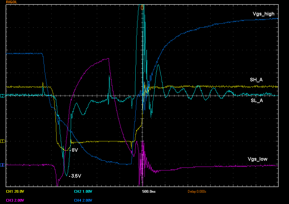
The issue is that the node between the FETs of the half-bridge drops to about -8V relative to the GND of my gate driver when the top FET turns off. I believe that this is largely due to the parasitic inductance of the circuit in combination with the very high current I am driving (~500A), aswell as the effect of the low-FET body diode beginning conduction. Now, this -8V relative to gate driver ground is bad for the SH_x pin of my gate driver and may be the reason I keep frying it. So, to solve this, I have installed a diode between the SH_x pin and gate driver ground, which keeps the SH_x pin from dropping below -0.7V. I also have a small 1Ohm resistor between the SH_x pin and the 'node' point between the two FETs to limit current through the diode when it is conducting.
The problem and this solution are summarized on page 12 of this document:
https://www.fairchildsemi.com/an/AN/AN-6076.pdf
So, the diode+resistor solved the negative transient on SH_x problem but has introduced another. Now, the high FET is slow to turn off resulting in large switching loss (heat). I believe this has occurred because if the high FET tries to turn off quickly (high di/dt), it's source voltage drops negative, increasing Vgs and slowing the turn-off. Since the gate driver cannot provide anything to the high FET gate below -0.7V, it is now limited in its ability to turn it off. This is my theory.
To alleviate this, I have put a 1ohm in series with the diode, which now allows a minimum of -3V on the SH_x pin. This has improved the situation a bit, acting as a compromise but it's not ideal.
I am looking for any comments or suggestions on how else I might go about fixing my problem.
Thanks.