timedate
Member level 5
Hi, all
I am using Altera Cyclone lV to receive the "LVDS" data from a clock and data recovery (ADN2813)
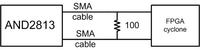
Below is my schematic,.
what I did in the PFGA is, let the pin work as "LVDS" or "LVDS bus", like below:

I can successfully receive the data. see "y7" and "rx", they are exactly the same(except the delay).

However, in the logic analyser, I found that, the signal would be suddenly comes to zero for a very short time. like blew.

Does anybody have idea, where this suddenly ZERO comes from? am I configure the FPGA as LVDS receiver correctly?
Besides, the LVDS signal is totally fine in the oscilloscope.
Thanks in advance.
I am using Altera Cyclone lV to receive the "LVDS" data from a clock and data recovery (ADN2813)
Below is my schematic,.

what I did in the PFGA is, let the pin work as "LVDS" or "LVDS bus", like below:

I can successfully receive the data. see "y7" and "rx", they are exactly the same(except the delay).

However, in the logic analyser, I found that, the signal would be suddenly comes to zero for a very short time. like blew.

Does anybody have idea, where this suddenly ZERO comes from? am I configure the FPGA as LVDS receiver correctly?
Besides, the LVDS signal is totally fine in the oscilloscope.
Thanks in advance.