Continue to Site

Welcome to EDAboard.com

Welcome to our site! EDAboard.com is an international Electronics Discussion Forum focused on EDA software, circuits, schematics, books, theory, papers, asic, pld, 8051, DSP, Network, RF, Analog Design, PCB, Service Manuals... and a whole lot more! To participate you need to register. Registration is free. Click here to register now.

Doubts on setting the bias Values of Vds ,Vgs,Ids, Igs for AVAGO ATF54143 transistor

Status
Not open for further replies.

pusparaga

Full Member level 4
Joined
Oct 19, 2013
Messages
197
Helped
4
Reputation
8
Reaction score
4
Trophy points
1,298
Activity points
2,988
Sir,
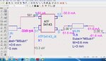
I took the Avago Technologies ATF54143 transistor to my work, I have chosen transistor of Vds =3V and Ids =60mA and am getting following values

(1) Vds= 3.00 V
(2) Ids =61.6mA
(3) Ig=1.82pA or sometimes getting 0 A ,when varying the resistors.

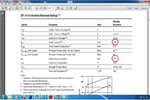
According to the transistor absolute maximum rating as follows

Vds = 5 v
Vgs= -5 to 1 v
Ids = 120 mA
Igs= 2mA

I have doubt on the Ig = 1.82pA, absolute maximum rating is Igs= 2mA. If I get this much low current at Gate, will transistor amplify it and also set Vds =3.00v and Ids =61.6mV. Is these values are o.k for biasing Vds =3v and Ids= 60mA.
Can you anybody clarify these doubts, I have attached obtained Vds , Igs and Vgs image and absolute maximum rating datasheet and also datasheet of ATF54143.
 

Attachments

  • Obtained_VDSandVGS.jpg
    Obtained_VDSandVGS.jpg
    230 KB · Views: 131
  • DataSheetValues.jpg
    DataSheetValues.jpg
    271.4 KB · Views: 113
  • ATF54143_avago_PHEMT.pdf
    136.8 KB · Views: 87

You confuse simulation results coming from the model and the reality..
"Max Rating" does not mean that the value will absolutely "be".Models can represent the device up to certain level and certain accuracy.This max. value has probably been measured and it's max-average real value.
In additional to this, Ig current representation in a model is less accurate, don't trust too much.
 
Dear Sir,
In the datasheet Igs absolute maximum can be upto 2mA. In my case I have got 1.82pA.My question is whether obtained Igs(1.82pA) correct or not. Also Ids= 61.6mA , I have got it. As I told you I took transistor biasing as Vds = 3v and Ids =60mA. I want clarify the obtained values of Ids, Vds and Igs in the posting #1, is it correct or not.

We cannot know that.. 2mA is a typical value as I have mentioned and 1.82pA is only Gate current coming from model and it does have an accuracy.It may be or not..
Ids vs. Vgs relation should be more accurate. Think about these values which are in data-sheet being as typical values.They have also a spread around this number.
But the model is just an approximation, it gives you the best results as much as possible but it is not absolute.
 
Ids vs. Vgs relation should be more accurate

BigBoss Sir ,
As you told, which relation should be more accurate either Vds vs Ids(this relation is given in the datasheet) or Ids vs Vgs( you said). I think, Ids vs Vds relation should be accurate. Please can clarify it.
 

The 2mA for Igs is the absolute maximum rating. It is the current magnitude that could potentially damage the device. You should not be simulating or operating anywhere near that current level.

If you are concerned about the current being low then you need to look at the bias network you have connected to the device. Does that have a configuration so that it can deliver greater levels of current at the required voltage range or are the resistors too high in value so that the current is limited by their values as allowing more current would yield greater voltage drop? Maybe you could reduce each resistance by some factor to keep the same voltage divide ratio but increase the available current and see what happens. Obviously though this would cause a decrease in the efficiency of the whole circuit.
 
I would say that Igs is mainly due to the electrons coming from the substrate and breaking the gate-source junction. this is called gate leakage current and it is highly undesirable because it damages the gate terminal of transistor so be happy if you are getting low enough leakage current.
 
Dear Sir,
One problem getting at the drain of the ATF54143 transistor, Some times at the DRAIN current showing -62.2mA,sometimes it is showing +62.2mA. As we know , there is no negative current, direction of the current is reversing.The current direction may change the polarity. As I told you, if -62.2 mA current appearing at the drain of the ATF54143 transistor, do we need to give attention or we have to make it appear current at the drain must be +62.2mA. Which is correct, even it appears -62.2mA at the drain, do we need bother or can we ignore it. Please can clarify it.
I have attached the following drain current at the ATF54143.
 

Attachments

  • DC_BIAS_SETTING_AT_VDS_IGS.jpg
    DC_BIAS_SETTING_AT_VDS_IGS.jpg
    461.6 KB · Views: 129

The positive or negative sign is important and cannot be ignored and also what you are seeing is absolutely correct. When DC annotation is added to a schematic it is written at a specific symbol pin and relates to the current at that pin with positive current flowing into the device through that pin and negative current flowing out of the pin. So when two devices are connected together with a single schematic wire and both end of that wire get DC annotation one end of the wire will have a negative current dues to the current flowing from the device to the wire and the other end will have a positive current due to the current flow from the wire to the device.
 
Status
Not open for further replies.

Part and Inventory Search

Welcome to EDABoard.com

Sponsor

Back
Top