Continue to Site

Welcome to EDAboard.com

Welcome to our site! EDAboard.com is an international Electronics Discussion Forum focused on EDA software, circuits, schematics, books, theory, papers, asic, pld, 8051, DSP, Network, RF, Analog Design, PCB, Service Manuals... and a whole lot more! To participate you need to register. Registration is free. Click here to register now.

How to shield Microstrip Line from Electronic Equipment or wires

Status
Not open for further replies.

soaringeagle

Junior Member level 3
Joined
May 25, 2013
Messages
30
Helped
0
Reputation
0
Reaction score
0
Trophy points
1,286
Activity points
1,514
I am designing a slot antenna that is fed by micro strip line.But I also need to shield the micro strip line from other electronics equipment that may come in contact with it. How can I achieve it ?

I do not want to use stripline.

An urgent help is required please.
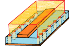
 

I am designing a slot antenna that is fed by micro strip line.But I also need to shield the micro strip line from other electronics equipment that may come in contact with it. How can I achieve it ?

I do not want to use stripline.

An urgent help is required please.

The effective width of the microstrip is \[w_eff=\frac{120{\pi}h}{ Z \sqrt{ \epsilon_eff}}\]
where \[\epsilon_eff=\frac{\epsilon+1}{2} + \frac{\epsilon-1}{2} {\left(1+\frac{10h}{w}\right)}^{-\frac{1}{2}}\]
(google the MS line calc for Z)

So, I think you should avoid putting anything in the area of \[(1\ldots2){\times}w_eff\] around the microstrip.
Outside you can put simple ground planes on the top layer. Or to be sure, put there a grid of vias with a step shorter than quarter-wavelength.

If your feeder is matched, you should not screen it on the top. However if it is a resonator of \[n \lambda/4\] (n>1), just put there a simple \[2w_eff{\times}3mm\] (w x h) grounded box on top to see how it works first.
 
Last edited:

My substrate is a rectangular box with 4 walls and is of certain thickness with no bottom and top wall . Just like a hollow rectangular box of certain thickness with no bottom and top wall. I have to protect the micro strip line that is etched on the inner side of my box. I have to put some equipment inside that hollow part of that box. So how can I avoid the radiation by the micro strip line affecting my S11 results?
 

My substrate is a rectangular box with 4 walls and is of certain thickness with no bottom and top wall . Just like a hollow rectangular box of certain thickness with no bottom and top wall. I have to protect the micro strip line that is etched on the inner side of my box. I have to put some equipment inside that hollow part of that box. So how can I avoid the radiation by the micro strip line affecting my S11 results?

sorry... I don't get it.
If it is a box, it should be 6 walls. If you tell me a planar topology, where's the top and the bottom?...

Tell me exactly, do you use a thin dielectric substrate where back plane is ground plane and other plane is a microstrip circuit? Because microstrip is just that - infinite ground plane and a strip wire separated by substrate layer with uniform ε .

Do you mean, you have an assembly frame with 4 walls, where the microstrip circuit is attached to one of the walls? Can you draw it?

Can you do like in the fig? It is done this way in some mobile phones.
1.gif
 
Last edited:

pic.png

I have attached the image file here. Kindly let me know , if it is still not clear.

- - - Updated - - -

I can understand your drawing and conceptually I have to do the same as you have shown in your drawing. But my geometry is different and I also have a slot etched on the ground ( ground is the outer part of my substrate as shown in attached figure). So if I connect anything through vias with ground , it will also affect the performance of my slot antenna. ( I think so).

So I need to keep the radiation of micstrostrip line reaching towards the outer side of my substrate ( because slot antenna is etched on it and causing the ground part to radiate ) but I have to suppress the backward radiation from microstrip because I have to keep some electronic circuitry there and i do not want it to come in contact with microstrip line ( also indicated in the attached figure).
 

I am sorry. It really looks complicated. First of all, if you have ground part affected by radiation - it looks as an answer, you can't do anything. The only option is to separate the microstrip circuitry... but if it is a simple line, why don't you use coaxial? It seems, you can't screen the electronics inside?
 

I am thinking of some solution, while keeping the micro strip line as it is designed in my diagram. :(.

- - - Updated - - -

or if somebody can tell me that best EM waves absorbing material that I can put on the back of my substrate to suppress radiation by the micro strip line ?
 

If I am not mistaken, you can't put an absorber directly on microstrip. The fringing fields actually extend not only to the sides, but above as well. You will get high loss and your impedance will change. And there are not much thin absorbers. Most of -6dB ferrite based sheet absorbers are narrow-band and rely on normal reflection from ground plane on the backside. In your case it is equivalent to simple screen box. And again, your ground plane actually is not ground... so I think you should avoid using it in the circuitry. I think, you should focus on the circuitry itself, how to isolate and screen it. There are specific on-chip absorbers on the market designed for cpu working conditions.
 
Last edited:

Thanks for your comments. I am not worried about the outer side of the substrate (ground) on which slot is etched. When I am using the stripline as feeding method for the slot , it is not giving me wider bandwidth. What can be possible reason for that ? With the microstrip , I am getting really good return loss and wider bandwidth , but only problem is to shield the microstrip using some technique.
 

Status
Not open for further replies.

Part and Inventory Search

Welcome to EDABoard.com

Sponsor

Back
Top