Continue to Site

Welcome to EDAboard.com

Welcome to our site! EDAboard.com is an international Electronics Discussion Forum focused on EDA software, circuits, schematics, books, theory, papers, asic, pld, 8051, DSP, Network, RF, Analog Design, PCB, Service Manuals... and a whole lot more! To participate you need to register. Registration is free. Click here to register now.

whether the bottom plate of a MOSCAP must be connected to gnd or VCC?

Status
Not open for further replies.

fightshan

Junior Member level 3
Joined
Jul 30, 2013
Messages
28
Helped
0
Reputation
0
Reaction score
0
Trophy points
1
Location
China
Activity points
260
picture1.png

picture2.png

In actual IC manufacturing,the two plates of a MOSCAP is not symmetrical.generally,the bottom plate should be connected to gnd(the lowest voltage in a chip,NMOSCAP) or VCC(the highest voltage in a chip,PMOSCAP).as shown in picture1,G is the top plate and B/S/D is the bottom plate.

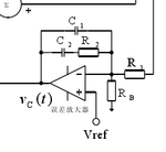
however,in the circuit of a integrator ,we need a cap which is connected between a input and the output as a feedback capacitor ,as shown in picture2 C1 and C2,so ,my question is : can i use the MOSCAP as the feedback cap?
 

can i use the MOSCAP as the feedback cap?

Depends, if you can get along with, or if you can avoid the C/V dependency, s. the following figure: View attachment PMOScap.pdf. The cap./area values given are for a 3.3V oxide thickness.

If you operate the PMOS in inversion mode (D,S,B+ , G- , normal PMOS operation), you need at least Vg=-Vth as difference voltage to make profit of the high cap./area ratio.

In accumulation mode (D,S,B- , G+) you can achieve even a little bit better cap./area ratio, but you need a pos. difference voltage of Vg >≈ 2|Vth| to make profit of it.
 
Status
Not open for further replies.

Part and Inventory Search

Welcome to EDABoard.com

Sponsor

Back
Top