Continue to Site

Welcome to EDAboard.com

Welcome to our site! EDAboard.com is an international Electronics Discussion Forum focused on EDA software, circuits, schematics, books, theory, papers, asic, pld, 8051, DSP, Network, RF, Analog Design, PCB, Service Manuals... and a whole lot more! To participate you need to register. Registration is free. Click here to register now.

clock distribution- calculating delays

Status
Not open for further replies.

nats_

Newbie level 6
Joined
Apr 12, 2012
Messages
14
Helped
0
Reputation
0
Reaction score
0
Trophy points
1,281
Activity points
1,378
Hi,
i have two questions on this topic:

1. how do i calculate a delay of certain component, if all i know is its' input capacitance?
(i have no knowledge of any resistance or even the lines' impedance).

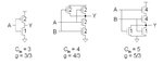
2. given a circuit with a DLL component (like in the image), how do i calculate the insertion delay?
Capture.PNG
thanks!
 

If you are talking about simple gates or simple path below might be helpful to you.

Delay has two components = Effort delay + Parasitic delay
D= F+P
where,
F= g*h ('g' is logical effort,'h' is Electrical Effort)

g = Capacitance of diffusion/ Capacitance of reference inverter
h = Capacitance of output/ Capacitance of input

P = Diffusion cap at output/ Diffusion cap of the reference inverter (Parasitic delay of a gate is the delay when gate drives at zero load).

Look at few examples in the picture.

Feel free to correct me if i am wrong.

FYI - These pictures are not owned by me. It is used just as a reference.
 

Attachments

  • Delay.jpg
    Delay.jpg
    28 KB · Views: 46
  • Logical-effort.jpg
    Logical-effort.jpg
    61.5 KB · Views: 43
  • Parasitic-delay.jpg
    Parasitic-delay.jpg
    53.3 KB · Views: 43

Status
Not open for further replies.

Part and Inventory Search

Welcome to EDABoard.com

Sponsor

Back
Top