Continue to Site

Welcome to EDAboard.com

Welcome to our site! EDAboard.com is an international Electronics Discussion Forum focused on EDA software, circuits, schematics, books, theory, papers, asic, pld, 8051, DSP, Network, RF, Analog Design, PCB, Service Manuals... and a whole lot more! To participate you need to register. Registration is free. Click here to register now.

Any input, a constant output.

Status
Not open for further replies.

ed_gops

Newbie level 3
Joined
Dec 8, 2013
Messages
4
Helped
0
Reputation
0
Reaction score
0
Trophy points
1
Location
Visakhapatnam
Activity points
34
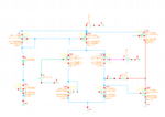
Hello everyone!!! I want a circuit which should produce a constant output voltage using MOS in cadence. I have done a design too, and its working fine. But I don't know whether it is acceptable for practical purpose or not. The design is done in 90nM CMOS Technology. The logic for the second stage for the image below is not clear. A NMOS is placed between the PMOS and NMOS of the inverter where the drain of two NMOS are connected together, so that there will be no effect of NMOS drain voltage change and a constant output (logic 1) is achieved upon any change in the input (for logic 1). Now the constant output 1.999V can be used to get any desired value at the output of the NMOS with diode connected PMOS load. Please, clarify me if this circuit is logically correct. If not send a design for the same requirement. Thanks in advance. comp1.png
 

Hi ed_gops,

In the circuit the NMOS in the middle arm is used as a capacitor. 1st inverter o/p is logic 0 so it turns ON the middle PMOS. The middle stage o/p is therefore almost VDD (1.199V). This turns on the last stage NMOS and a constant current is drawn. As the last stage PMOS is diode connected the O/P is constant at VDD-Vsg (which in this case is 0.6V).

For experiment purpose this is fine. But practically there are limitations to this circuit.
In real scenario we have some thing called PVT (Process voltage and Temperature). With variation in PVT the O/P will vary over a wide range (20%-30% approx). It is recommended to have a proper negative feed back loop to get a fixed output. More over you cannot have any desired o/p from this ckt. The o/p is fixed at VDD-Vsg.

Hope this will help .. :)
 

Thank you very much Siddharth Hazra sir for your help. Actually, I wanted to make a circuit which produces a constant 600mV at its output while any AC input(ranges from 200mV to 900mV) is applied. Also there should not be any change in the AC components like magnitude amplitude or frequency(should be as it is at the input).This output(600mV) will become input for my Opamp. So, any DC voltage change in the signal line should not affect the Opamp performance, in short effect of DC Offset voltage cancellation. If you have any suggestion or any circuit configuration, please provide that to me.
I have other doubts too. My Opamp is a basic two stage opamp, shown bellow. My question is, why should we provide VDD/2 at input and set VDD/2 at output? And is it mandatory that the current should be same at both the stages? For what purpose these configuration has to be set, and Actually how the configuration should be for a two stage Opamp? Thank you siropamp-schematic.png.
 

Status
Not open for further replies.

Part and Inventory Search

Welcome to EDABoard.com

Sponsor

Back
Top