Continue to Site

Welcome to EDAboard.com

Welcome to our site! EDAboard.com is an international Electronics Discussion Forum focused on EDA software, circuits, schematics, books, theory, papers, asic, pld, 8051, DSP, Network, RF, Analog Design, PCB, Service Manuals... and a whole lot more! To participate you need to register. Registration is free. Click here to register now.

Power Efficiency Calculations of Switched Capacitor DC-DC Converter

Status
Not open for further replies.

DimaKilani

Member level 1
Joined
Jan 23, 2014
Messages
39
Helped
0
Reputation
0
Reaction score
0
Trophy points
1,286
Activity points
1,648
Hi everyone,

I'm designing a step down Switched Capacitor (SC) dc-dc converter. I'm using a spice simulation in order to observe the behavior of the circuit.

I want to calculate the power efficiency of the SC converter. efficiency=Pout/Pin. pout=Iou*Vout which is constant.

The problem here is the Pin since the current is fluctuating between negative microAmpere and positive microAmpere. So, in order to calculate the input power efficiency, I used the 1/T*integral (V*I). if we think about the integral, it means the area under the curve. this means that some negative values of the input power will cancel the positive values. and that will affect the power efficiency. Am afraid about this point.

Anyone has an idea about this problem. Is the input current of the of the SC converter is varying ? or maybe my design is wrong ..

Thanks,
Dima
 

I would assume the converter is powered by a single DC supply. It that case the current will always be positive (or uni-directional). How do you get negative current?
 

Yes, I use one DC power supply for the: 1)input converter 2)clock of the converter 3)the PMOS and NMOS transistors of the converter

I am also wondering where is negative current come from!

Thanks
 

Your schematic is a little fuzzy so it's hard to read, but I suspect that any negative current spikes are due to capacitive coupling from the drive signals. What is the magnitude and duration of the negative spikes?
 

So, in order to calculate the input power efficiency, I used the 1/T*integral (V*I). if we think about the integral, it means the area under the curve. this means that some negative values of the input power will cancel the positive values. and that will affect the power efficiency. Am afraid about this point.
You are asking about the efficiency measurement, not for opinions about the circuit design. In so far, yes the measurement is right. Because Vin is constant, Pin calculation can be further simplified to Vin*avg(Iin). For an exact efficiency determination, you may want to include the clock driver supply current.
 

Mmm Actually, the duty of the negative input current is high a little bit, but am afraid that when am going to implement it as IC, I will not have a negative current in reality as in the simulation.

what about if I took the absolute value of the input current? I took the abs(Iin), that actually will increase the input power and decrease the power efficiency.

- - - Updated - - -

In other words, can I have negative current when testing the SC converter as IC ? or it just appears in the simulation only ?

- - - Updated - - -

Also, yup I included the gate drive power in my calculation.

- - - Updated - - -

Your schematic is a little fuzzy so it's hard to read, but I suspect that any negative current spikes are due to capacitive coupling from the drive signals. What is the magnitude and duration of the negative spikes?

The maximum negative current is -80microA and it increases to reach +80microA.
 

what about if I took the absolute value of the input current? I took the abs(Iin), that actually will increase the input power and decrease the power efficiency.
Absolute value and it's average have no physical meaning in this case. You are looking for average current which corresponds to the average input power.

In other words, can I have negative current when testing the SC converter as IC ? or it just appears in the simulation only ?
You shouldn't worry about it. I assume there will be negative current spikes in the real circuit, but also a bypass capacitor that filters current spikes.
 

Can you insert a low-ohm resistor at your power supply, and have the simulator give you a reading of power through it? In absolute watts.

You still may need to estimate an average value from the waveforms. Then convert to amperes.

As for negative current flow, does any charged capacitor have a path to discharge back through the supply at any time?
 

Dima, why did you delete the post with the circuit diagram? (Previous post #5).

Looks like a pretty strong hint that we should stop further contributions.
 

Now, let us sum up our discussion. I'm designing a switched capacitor dc-dc converter. I end up with negative current which is not a big issue as you mentioned. and You said, my power calculations are right as I use : Pavd = 1/T*integ (Iin*Vin).

The problem is that I noticed that the off current is too high which is in microA but am expecting to be in nanoA. when i tested the current of the transistor, I found that there is a high gate leakage current. I dont know where is the leakage come from and I dont know how to solve it.

It is just a simple dc-dc converter and no one in the literature review mentioned about this problem !!

- - - Updated - - -

but negative current means a reverse current in the circuit and it either go back to the battery or it go as a leakage which will affect my efficiency .. or what do you think ?
 

No circuit to discuss...

It looks like you are erroneously counting capacitive gate currents as "leakage".
 

here it is
SC_1.PNG

- - - Updated - - -

gate are re[laced by NMOS and PMOS transistor

- - - Updated - - -

sorry, I mean the switches are replaced by PMOS and NMOS transistor
 

* When I get inexplicable current flows in a simulation, it is often cured by reducing the time step.

* There is a chance the simulator may (mistakenly) overlap clock transitions on capacitors. They can discharge slightly during that iteration.

* The simulator may not care about tiny currents in the nA range, and will say 'we did enough iterations, the circuit has converged, let's call the frame done.'

* Is there any load attached? The slightest load will keep the supply providing positive current.

Actually, yes there is a load at the output, but it didnt solve the issue. My problem is that i observed that there is a gate leakage in the transistor of the switched capacitor circuit where a large amount of the current goes from the source to the gate. I simulated the transistor standalone in order to observe the gate, source and drain current, but i see no gate leakage which is expected.

I thought that the capacitors may causes that leakage, so what i did is I added a capacitor with the standalone transistor and again measure the current. but again, i see no leakage.

I dont know where is the leakage come from ?! what do you think ?

- - - Updated - - -

by the way, am using cadence tools with 65nm process technology
 

The term gate "leakage" involves an average current through the gate. Do you actually see a leakage current? As far as I remember your previously posted circuit and related measurements, you have been reporting pulsating currents but not specifically leakage currents.
 

here it is
View attachment 101742

- - - Updated - - -

gate are re[laced by NMOS and PMOS transistor

- - - Updated - - -

sorry, I mean the switches are replaced by PMOS and NMOS transistor
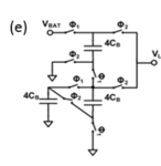
In looking at that circuit, it seems that with ideal no-loss switches, the efficiency would approach 100% for loads approaching zero Amps. It looks like it is designed to produce a voltage that is exactly 2/3 of the battery voltage. The lower two capacitors will both charge up to 1/3 of Vbatt and the upper capacitor will charge to 2/3 of Vbatt during phase 1. Then during phase 2, the lower two capacitors will be connected in series to produce 2/3 Vbatt and this combination will be placed in parallel with the upper capacitor, which also is at 2/3 of Vbatt. Everything is so well balanced that no current needs to flow when there is no load.

Notice also that this circuit, all by itself, does not produce a DC voltage. It still needs some filter caps. Since you have not shown any way for power to be wasted (other than imperfect switching), I don't see how you expect to find any meaningfull calculation of efficiency with a simulation.
 

The term gate "leakage" involves an average current through the gate. Do you actually see a leakage current? As far as I remember your previously posted circuit and related measurements, you have been reporting pulsating currents but not specifically leakage currents.

Yes, I see a gate leakage. When I measured the current across the transistor, large amount of the source current goes to the gate.

- - - Updated - - -

be aware that i replaced the switches by NMOS and PMOS transistor with 65nm process technology. This means that the circuit is not ideal. Yes, I added a capacitor load at the output in order to reduce the voltage ripples.

As you mentioned when explaining the operation, in the 1st phase, the input current (on current of the switched capacitor) will charges the capacitors. in the 2nd phase, the supply will disconnected from the capacitors, and the then the capacitor will discharge into the load. This means that the input current (off current of the switched capacitor) should be almost zero because the supply is disconnected in the 2nd phase. But what i got in my simulation is that there is an off current which is near to the on current that is in microA. I tried to figure out the problem why the off current is high. So, i measured the source, drain, gate and bulk current and I found there is a leakage current goes from a source to the load. I dont know how to solve such issue.

The current in the 2nd phase should be almost zero because the supply is disconnected. Am I right ?

- - - Updated - - -

be aware that i replaced the switches by NMOS and PMOS transistor with 65nm process technology. This means that the circuit is not ideal. Yes, I added a capacitor load at the output in order to reduce the voltage ripples. The circuit works properly and I tested each voltage node and it gives me the expected voltage as what I analyze it theoretically.

As you mentioned when explaining the operation, in the 1st phase, the input current (on current of the switched capacitor) will charges the capacitors. in the 2nd phase, the supply will disconnected from the capacitors, and the then the capacitor will discharge into the load. This means that the input current (off current of the switched capacitor) should be almost zero because the supply is disconnected in the 2nd phase. But what i got in my simulation is that there is an off current which is near to the on current that is in microA. I tried to figure out the problem why the off current is high. So, i measured the source, drain, gate and bulk current and I found there is a leakage current goes from a source to the load. I dont know how to solve such issue.

The current in the 2nd phase should be almost zero because the supply is disconnected. Am I right ?

- - - Updated - - -

In looking at that circuit, it seems that with ideal no-loss switches, the efficiency would approach 100% for loads approaching zero Amps. It looks like it is designed to produce a voltage that is exactly 2/3 of the battery voltage. The lower two capacitors will both charge up to 1/3 of Vbatt and the upper capacitor will charge to 2/3 of Vbatt during phase 1. Then during phase 2, the lower two capacitors will be connected in series to produce 2/3 Vbatt and this combination will be placed in parallel with the upper capacitor, which also is at 2/3 of Vbatt. Everything is so well balanced that no current needs to flow when there is no load.

Notice also that this circuit, all by itself, does not produce a DC voltage. It still needs some filter caps. Since you have not shown any way for power to be wasted (other than imperfect switching), I don't see how you expect to find any meaningfull calculation of efficiency with a simulation.


be aware that i replaced the switches by NMOS and PMOS transistor with 65nm process technology. This means that the circuit is not ideal. Yes, I added a capacitor load at the output in order to reduce the voltage ripples. The circuit works properly and I tested each voltage node and it gives me the expected voltage as what I analyze it theoretically.

As you mentioned when explaining the operation, in the 1st phase, the input current (on current of the switched capacitor) will charges the capacitors. in the 2nd phase, the supply will disconnected from the capacitors, and the then the capacitor will discharge into the load. This means that the input current (off current of the switched capacitor) should be almost zero because the supply is disconnected in the 2nd phase. But what i got in my simulation is that there is an off current which is near to the on current that is in microA. I tried to figure out the problem why the off current is high. So, i measured the source, drain, gate and bulk current and I found there is a leakage current goes from a source to the load. I dont know how to solve such issue.

The current in the 2nd phase should be almost zero because the supply is disconnected. Am I right ?

- - - Updated - - -

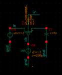
here i use the pmos as a switch and i connected a capacitor to it. (note: V/15/MINUS) is the input current.

There is no leakage current in this case when both pmos on and off. but in my Switched capacitor circuit, there is a leakage although i use same transistor size and capacitor.

But i noticed that the input current has negative and positive values, it there any reason for that?
schematic2.PNGsim1.PNGsim2.PNGsim3.PNGsim4.PNG

- - - Updated - - -

becuase you mentioned something about the ideal switches. I designed before a switched capcitor with a gain of 1/2 with ideal switches. and I would like to share it with you.

and the results are expected where the input current when S1 is on in microA, when when S1 is off which means the off current is in femtoA.

but when replacing the ideal switches with the pmos and nmos transistors, the off current becomes in uA (uA=microA).
schematic3.PNGsim5.PNGsim.PNG

- - - Updated - - -

Any ideas ?

Your help is highly appreciated :)
 

The term gate "leakage" involves an average current through the gate. Do you actually see a leakage current? As far as I remember your previously posted circuit and related measurements, you have been reporting pulsating currents but not specifically leakage currents.

Does choosing the type of transistor affect the leakage ? I mean I used PMOS and NMOS and replaced randomly instead of the ideal switches ?
 

Does choosing the type of transistor affect the leakage ? I mean I used PMOS and NMOS and replaced randomly instead of the ideal switches ?
Are you driving the gates so that they are sometimes forward biased? If so, that is your problem. The gate of an enhancement mode FET must always be driven to either the same voltage as the source pin, or else in the direction of enhancement with respect to the souce pin. If you can't ensure that, the gate will take current, and it is not considered "leakage". It is considered forward biased, and it is improper design.
 

Status
Not open for further replies.

Part and Inventory Search

Welcome to EDABoard.com

Sponsor

Back
Top