Continue to Site

Welcome to EDAboard.com

Welcome to our site! EDAboard.com is an international Electronics Discussion Forum focused on EDA software, circuits, schematics, books, theory, papers, asic, pld, 8051, DSP, Network, RF, Analog Design, PCB, Service Manuals... and a whole lot more! To participate you need to register. Registration is free. Click here to register now.

In ADS, How to generate the layout for two parallel connected VIA2 grounds.

Status
Not open for further replies.

raju_kambar

Full Member level 3
Joined
Jun 19, 2013
Messages
153
Helped
5
Reputation
10
Reaction score
5
Trophy points
18
Location
Earth
Activity points
1,404
Dear Sir,
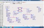
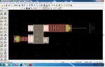
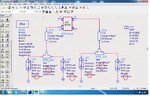
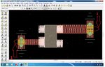
I have connected two parallel VIA2 grounds to sources of the transistor ATF54143. I want to generate the two parallel connected two VIA2 grounds. Just I have connected two VIA2 grounds simple manner, I didn't use any MTEE and MCORN to connect parallel two VIA2 grounds.Just connected and generated layout, Two parallel VIA2 grounds are not all appearing parallel in generated layout. Can you advice to me , what we have to use for generation of two parallel VIA2 grounds , what I need to use for separation of two VIA2 and they should appear separately in the layout , which bend , corner , I have to use and generate. Please can you help me.Here with,I am attaching the Schematic and layout generation of two parallel connected VIA2s.
 

Attachments

  • Parallel_two_via2_SCHEMATIC.jpg
    Parallel_two_via2_SCHEMATIC.jpg
    594.9 KB · Views: 119
  • Parallel_Two_VIA2_LAYOUT_Generation.jpg
    Parallel_Two_VIA2_LAYOUT_Generation.jpg
    610.5 KB · Views: 98

Dear Sir,
Please help someone else to resolve this difficulty.
 

Sir,
They may be coincided, what we have to connect to separate the two parallel VIA2 ground. They must be automatically separate,when we generate layout. What bend, MCORN, MTEE, we have to use. We should not manually move to separate two parallel VIA2 grounds.Can you tell me.
 

If you want the layout to be generated automatically without any manual adjustment then you must make sure that you never connect more than two symbols pins together at one connection. That means transistor pin to MLIN pin, MLIN pin to a single VIA2 pin, etc and never MLIN pin to 2 VIA2 pins. So you need to add something that creates two "output" pins from a single "input" pin. Therefore an MTEE with middle pin connected to the MLIN and the 2 opposite pins each connected to a single VIA2.

If the length of the transmission line is tuned then you will need to adjust (shorten) its length to compensate for the additional "length" in the layout of the MTEE. You will also have to adjust the length of the MLIN further to compensate for the "length" added by the connected VIA2 elements.
 
Therefore an MTEE with middle pin connected to the MLIN and the 2 opposite pins each connected to a single VIA2.

If the length of the transmission line is tuned then you will need to adjust (shorten) its length to compensate for the additional "length" in the layout of the MTEE. You will also have to adjust the length of the MLIN further to compensate for the "length" added by the connected VIA2 elements.

RealAEL Sir,
Thank you for your help, I am sorry that I didn't understand, what you said in the previous post , can you it show diagrammatically. How we can connect the two VIA2 parallel and generate layout. After layout generation, we shouldn't manually drag and separate it the two VIA2 in the layout, parallel connection of two VIA2 come automatically in the layout. Can you show it diagrammatic connection, how we can get it sir. If we use SINGLE VIA2 instead of two parallel VIA2,we will loose overall gain of the amplifier like anything.
 

As soon as you try to place the appropriate components in the schematic is should become obvious.

Code:
     Transistor
         |
       MLIN
         |
VIA2 - MTEE - VIA2
Physically they are connected in parallel even if in the schematic they are not directly wired in parallel with each other.
 
.

Code:
     Transistor
         |
       MLIN
         |
VIA2 - MTEE - VIA2
.

RealAEL Sir,
As you have shown in the code, I connected and generated the layout. For MTEE widths W1 and W2 , I am taking the adjacent VIA2 ground widths. Is it correct sir, whatever I have generated layout from the schematic , I have shown below, please make it confirm sir, weather it is correct or not (both schematic and layout).

As I have shown in the generated layout figure. at the arrow mark 1 shown in figure, there is no gap appearing between two VIA2 (Is it O.K or there must be gap between two VIA2 ground) . At the arrow mark 2 shown in figure, there is gap between two VIA2.
Here with I am attaching both schematic and generated layout.
 

Attachments

  • Parallel_two_via2_SCHEMATIC_1.jpg
    Parallel_two_via2_SCHEMATIC_1.jpg
    666.5 KB · Views: 116
  • Parallel_Two_VIA2_LAYOUT_Generated_1.jpg
    Parallel_Two_VIA2_LAYOUT_Generated_1.jpg
    784.7 KB · Views: 115

I cannot say whether anything is right or wrong. You, as the designer, are the only one who can make that decision. Is the design configuration as required? Does it yield the correct simulation performance? Is it manufacturable or does any part of the design violate some limit set by the board manufacturer? These are questions that you need to answer yourself to say whether the design is good or bad.
 
Status
Not open for further replies.

Part and Inventory Search

Welcome to EDABoard.com

Sponsor

Back
Top