Continue to Site

Welcome to EDAboard.com

Welcome to our site! EDAboard.com is an international Electronics Discussion Forum focused on EDA software, circuits, schematics, books, theory, papers, asic, pld, 8051, DSP, Network, RF, Analog Design, PCB, Service Manuals... and a whole lot more! To participate you need to register. Registration is free. Click here to register now.

Altium: still on custom pad creation, merging 2 pads

Status
Not open for further replies.

CiccioB

Newbie level 4
Joined
Dec 30, 2013
Messages
5
Helped
2
Reputation
4
Reaction score
2
Trophy points
3
Activity points
72
Hello,
I have looked for a solution to this problem everywhere, but I could not find any solution.

I am trying to create a custom footprint with some custom pads. These pads are nothing special: they are a joining of 2 elementary pads. One pad is only on the top layer, the second is a multilayer pad, so it has a hole.
The idea is to have a SMD footprint with added pass-through pads at the SMD pads extremes.

However I cannot find a way to connect those 2 pads. Even if they have the same designator number and Jumper ID, you cannot overlay them, nor you can add a trace between them. Once you use the footprint in PCB designer, you have lots of short circuit warnings.

The only workaround to this limitation is to keep the pads separated and then join them in PCB designer. Which is not really elegant nd you can't achieve the wanted pad form.

A am missing something or Altium Designer cannot understand when two pads are the same and thus apply to each of them the entire project rules so it detects short circuits, clearance and all other rule violations?
It is really not comfortable to go and create an exception rule for each footprint created and added to the design with such "double" pads. So there's some other workaround for this limitation?

Thanks in advance
 

hi.do you want to have 2 pad in 2 layer(top and bottom ) in away that they connect to each other.if yes, have you try the via instead of pad?
 

hi.do you want to have 2 pad in 2 layer(top and bottom ) in away that they connect to each other.if yes, have you try the via instead of pad?

Thanks for the answer.
Yes, I did. Via is not different than a normal PAD. Still short circuits are reported when using them.

Here an example.
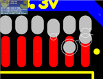
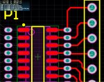
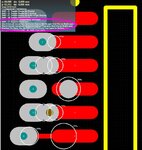
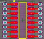
First how the pads have been defined in the footprint editor:

Footprint_zps6fac8219.png

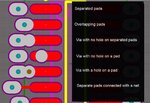
And here the errors reported by the PCB designer

Designer_Error_zps4d53da2f.png

As you can see the only way to not have errors is to design two separate pads that have to be joined with a track in the designer. And that still works only if the pad is assigned to a net. If you try to place a footprint in your project as a mechanical object (so it is not linked to schematics), you still cannot join the tracks.
I find it quite silly. But again, it may be me that is missing something.

/edit: hole layer has been hidden in PCB designer, but pads and vias holes are there, trust me ;)
 
hi
i want know are you create new footprint with surface pads and through hole pads?
if u want have a component with 2 package, you should create new footprint in PCB Library Editor Like this
**broken link removed**
attention to pad designators(all of them should twines)
add your footprint to mentioned component in SCH editor
update your pcb
finally OUTCOME
**broken link removed**
 

Hi,
yes, the intention is to have a footprint that adapts SMD components to thru-hole pads.
I made my footprint in PCB library (my first pic in my previous post). However those footprint are not associated to any net as they are only mechanical footprint that are added to the board but not part of the schematics.
In that case separate pads with same ID do not work because without a net connecting pads you cannot trace nets between SMD pads and thru-hole pads. Designer forces routing to avoid pads, even though they have the same identifier as part of the same footprint.

I see this as a big limitation in Altium Designer, as pads with same identifier should be threated as a single object and not as separated ones to which apply the clearance and short circuits checks.
I hoped the problem was me, but as far as I understand, the problem is in the tool.

Thanks nevertheless.
 

...the intention is to have a footprint that adapts SMD components to thru-hole pads...

This problem can be turned around by using Vias working as Tracks, just changing its layer from default Multilayer to Toplayer and assigning the same pin designator to both. And, of course, setting its Hole Size parameter to "0".

Depending on footprint complexity, this drawing will be an exhaustive task, but already worked for me.


+++
 

hi
However those footprint are not associated to any net as they are only mechanical footprint that are added to the board but not part of the schematics.
In that case separate pads with same ID do not work because without a net connecting pads you cannot trace nets between SMD pads and thru-hole pads
is your purpose add a free footprint after net list loading to your board?
if this is your problem u most assign mentioned nets to mentioned pads
3.jpg
if you do this you can trace mentioned pads much as on your footprint pads aren't twins and they names are different.
 
This solution seems concern to routing scope.
What he want is to perform this association on library scope.


+++
 

i draw line between pads on pcb library editor and place it on pcb sheet and dont have any error
no clearance error, no short circuit error
is this on library scope?
 
Last edited:
This solution seems concern to routing scope.
What he want is to perform this association on library scope.

Mmm, no, it's not a routing problem. Routing is a problem because the footprint ignores same pads with same identifier. Or I can't make it recognize them as a single split pad.
If the footprint would manage the pads as it should there should not be any need for routing the footprint pads to themselves.

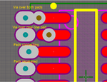
Here again a test adding the suggestion that some of you made:

Footprint.jpg
Designer.jpg

I hope you can see the attachments, otherwise I'm going to link them from an external image host provider.

Nets and vias don't seem to make any difference or providing a workaround to the problem.

i draw line between pads on pcb library editor and place it on pcb sheet and dont have any error
no clearance error, no short circuit error
is this on library scope?
Sorry I could not understand what you did exactly. Did you draw a net between pads in the library? Have you tried placing the resulting footprint on the PCB and see what happens?
I drew a net between separated pads with same identifier and the results are as shown on the image above.
What do you mean with "library scope"?

What I would like is a footprint that encapsulates all connections between pads so that I do not have to put a dummy component in the schematics and then connect all pads pair one at a time each of them.
As ask if this is possible and it is me that is not able to achieve that, or that Altium footprint library has this limit (quite silly from the point of view of functionality, quite sever under the point of view of the limitations it introduces). Looking at those presentations it seems that this tool makes anything one may think about with stunning 3D presentations. I cannot believe it cannot route correctly two pads in footprint library. It must be me.
 
...Nets and vias don't seem to make any difference or providing a workaround to the problem...

I could not see exactly what was suggested on figures above.
The procedure consists to connect not a track to a via, but a via to another via, which have the same pin designator.

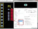
Note that the trick is change the layer of via from default Multilayer to Toplayer, and resize its hole to zero. You can also observe that now the via appears as a track and you are able to associate a pin designator to this "track" which was build from a via.

i draw line between pads on pcb library editor and place it on pcb sheet and dont have any error
no clearance error, no short circuit error
is this on library scope?

The problem is that we can´t associate a designator number to a track during PCB library edition, and after update to board and perform DRC check on layout, this connection is incorrectly perceived by Altium as a short-circuit.

If worked with you, perhaps you are executing some step we had missed.


+++
 

i think u have a pcb document and load net-list on this and add that footprint on your doc after loading net-list.
that is fault
after loading net-list all of copper layers checked by DRC(Design Rule Check) so when you add a new footprint on pcb doc ,added footprint pads dont have any connections.so in this case all of footprint pads shouldn't have any connection to other pads.even to itself pads.because all of it pads is free.
if you add your footprint to component on SCH doc you don't have any problems.
or when you add new footprint on pcb doc for pads assign nets.even for this footprint:
6.jpg
this problem don't relate to tool.
in all of pcb designer softwares that have online error rules check event grew thats action to avoid any short circuit problems.
 
I could not see exactly what was suggested on figures above.
The procedure consists to connect not a track to a via, but a via to another via, which have the same pin designator.

Note that the trick is change the layer of via from default Multilayer to Toplayer, and resize its hole to zero. You can also observe that now the via appears as a track and you are able to associate a pin designator to this "track" which was build from a via.

Hi again,
I've tries to do some test but it seems the tool doesn't allow me to change default via layer from multilayer to any single layer mode. I've put the hole size to zero and I have also tried to force single layer mode by setting start and layer to the same layer, but that doesn't work.
It seems I'm stuck with a multilayer via that cannot be connected to anything in PCB library unless I want a short circuit :-x

I think at the end I'll create a rule footprint related so that I can put holes as near as needed to pads without creating a shortcut.

Thanks

- - - Updated - - -

i think u have a pcb document and load net-list on this and add that footprint on your doc after loading net-list.
that is fault
after loading net-list all of copper layers checked by DRC(Design Rule Check) so when you add a new footprint on pcb doc ,added footprint pads dont have any connections.so in this case all of footprint pads shouldn't have any connection to other pads.even to itself pads.because all of it pads is free.
if you add your footprint to component on SCH doc you don't have any problems.
or when you add new footprint on pcb doc for pads assign nets.even for this footprint:
View attachment 101160
this problem don't relate to tool.
in all of pcb designer softwares that have online error rules check event grew thats action to avoid any short circuit problems.
Hi,
unfortunately even if I add a component with my doubled-pads footprint to schematics on PCB short-circuits are always detected.
 

Originally Posted by CiccioB
Hi,
unfortunately even if I add a component with my doubled-pads footprint to schematics on PCB short-circuits are always detected.
i dont have any problems for created footprint or ERC on pcb sheet. i think your software have problem.
do you C-Rack altium designer?
 

Status
Not open for further replies.

Part and Inventory Search

Welcome to EDABoard.com

Sponsor

Back
Top