Mryemeni
Newbie level 6
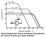
In microchip application note AN236, a 4069 inverter is used as an amplifier in the receiver, and I can't understand the reason for that.
I tryed to simulate the inverter as it shown in the datasheet with feedback resistor using LTspice but that didn't get me anywhere, can anyone help me understand the workings of such design choice.
Thanks in advance.
I tryed to simulate the inverter as it shown in the datasheet with feedback resistor using LTspice but that didn't get me anywhere, can anyone help me understand the workings of such design choice.
Thanks in advance.