carl_chao
Member level 3
Hi,
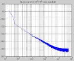
I just wrote a time-domain PLL behavior model including VCO phase noise and non-idealities from other blocks. I have generated the time-domain open-loop VCO 1/f^3+1/f+white phase noise as shown below:

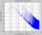
In the PLL time-domain behavior model, I inserted the above VCO open-loop phase noise at the output of the VCO according to this reasoning: At the current calculation time step, test if the phase of the VCO output is at or crossing 0 or N*2*pi (N is an integer). If yes, then insert this noise into the VCO output phase. After doing this (with all other non-idealities switched to ideal), I got the phase noise of the PLL as following:

As you can see from this figure, the high-frequency phase noise of the open-loop VCO directly showed up in the PLL output, while the low-frequency part was suppressed.
Now, my question is, whenever I put the VCO into ideal or changed VCO open-loop phase noise to white noise only, the phase noise curve of the PLL output would be very smooth (i.e., without any spurs as shown in the 2nd figure, but certainly with white noise, the noise floor increased). But whenever I added 1/f^3 and/or 1/f noise to the VCO, these spurs would show up. The frequency of the lowest spur is at the PLL input reference frequency, and all others are at its multiples. If these spurs are real, or just errors due to my modeling method?
If these spurs are real, I wonder if I can give the following explanation: after adding the 1/f^3 and/or 1/f noises, because of the near DC nature of these noises, at each input reference clock period, the charge pump mostly needs to put out a same-polarity pulse to compensate this DC bias, in an effort to align the frequency of the VCO with that of the reference input. This process is equivalent to having a charge-pump with mis-matched up-down currents, which we know will give rise to reference leakage to the output.
I just wrote a time-domain PLL behavior model including VCO phase noise and non-idealities from other blocks. I have generated the time-domain open-loop VCO 1/f^3+1/f+white phase noise as shown below:

In the PLL time-domain behavior model, I inserted the above VCO open-loop phase noise at the output of the VCO according to this reasoning: At the current calculation time step, test if the phase of the VCO output is at or crossing 0 or N*2*pi (N is an integer). If yes, then insert this noise into the VCO output phase. After doing this (with all other non-idealities switched to ideal), I got the phase noise of the PLL as following:

As you can see from this figure, the high-frequency phase noise of the open-loop VCO directly showed up in the PLL output, while the low-frequency part was suppressed.
Now, my question is, whenever I put the VCO into ideal or changed VCO open-loop phase noise to white noise only, the phase noise curve of the PLL output would be very smooth (i.e., without any spurs as shown in the 2nd figure, but certainly with white noise, the noise floor increased). But whenever I added 1/f^3 and/or 1/f noise to the VCO, these spurs would show up. The frequency of the lowest spur is at the PLL input reference frequency, and all others are at its multiples. If these spurs are real, or just errors due to my modeling method?
If these spurs are real, I wonder if I can give the following explanation: after adding the 1/f^3 and/or 1/f noises, because of the near DC nature of these noises, at each input reference clock period, the charge pump mostly needs to put out a same-polarity pulse to compensate this DC bias, in an effort to align the frequency of the VCO with that of the reference input. This process is equivalent to having a charge-pump with mis-matched up-down currents, which we know will give rise to reference leakage to the output.