Continue to Site

Welcome to EDAboard.com

Welcome to our site! EDAboard.com is an international Electronics Discussion Forum focused on EDA software, circuits, schematics, books, theory, papers, asic, pld, 8051, DSP, Network, RF, Analog Design, PCB, Service Manuals... and a whole lot more! To participate you need to register. Registration is free. Click here to register now.

A question about the floating bandgap reference in Razavi's book

Status
Not open for further replies.

Hamid.Kiumarsi

Full Member level 2
Joined
Aug 18, 2010
Messages
142
Helped
33
Reputation
66
Reaction score
31
Trophy points
1,308
Location
Japan
Activity points
2,232
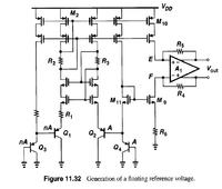
The schematic of this floating reference is at the end of chapter 11 of Razavi's CMOS book. (please refer to the attached file)
I am having a hard time to understand why Vgs9 = Vgs11. Based on this fact we Razavi has deduced that the voltage drop on R6 equals VBE4.
If Vgs9=Vgs11, then according to the fact that he assumes that M9 and M11 are identical, we should have ID9 = ID11
and since all emitter currents of Q1-Q4 are equal, then we would have ID9 = ID11 =====>>VBE4/R6 = (2Vt*ln(n))/R1
The problem is: then Vout = (R4/R6)*VBE4 + 2(R5/R1)*Vt*ln(n) ====>> Vout = (R4+R5) * (2Vt*ln(n))/R1 or Vout = (R4+R5) * VBE4/R6

Where do I make a mistake?

Is ID9 = ID11?


Vout = (R4/R6)*VBE4 + 2(R5/R1)*Vt*ln(n) ====>> Vout = (R4+R5) * (2Vt*ln(n))/R1 or Vout = (R4+R5) * VBE4/R6

Where do I make a mistake?
No mistake, I think, just a different presentation. But it doesn't contain the 2 counter-running temperature dependencies of VBE4 and Vt, which are necessary to calculate the correct resistance ratios (R4/R6) and 2(R5/R1) corresponding to the ratio of their respective temperature dependencies, in order to achieve a best-possible compensation at a selected temperature.

Is ID9 = ID11?
Yes. The right choice of resistors within the limits of the resistor ratios given above should make this possible.
 

Then what mechanism in the circuit makes Vgs9 = Vgs11 possible?
If there was no opamp and node E and F were connected together, current mirrors would result in ID9 = ID11 which inturn leads to Vgs9 = Vgs11 (of course with the right choice of transistor's dimensions)
But now that node E and F are disconnected, the only information we have is VE = VF.
If VF remains the same before and after putting opamp in place, then we can conclude that opamp has no effect on ID9 or ID11 and they remain equal.

I seem to be a little bit lost in here.
 

If VE=Vf & R4=R5, then the current through M10 & M9 are the same & So is M11 &M10 currents -->making Vgs9=vgs11. And lets assume Vgs9 >Vgs11. Then we will have node Ve not equal to Vf, which is not possible with the amp.
 

If VE=Vf & R4=R5, then the current through M10 & M9 are the same & So is M11 &M10 currents -->making Vgs9=vgs11. And lets assume Vgs9 >Vgs11. Then we will have node Ve not equal to Vf, which is not possible with the amp.
Actually R4 is not equal to R5; see the original paper which proposed this topology: "A Low-Power Differential CMOS Bandgap Reference" by T. Brooks et al
Moreover, we have Vout = R5*ID10 + R4*ID9 + VEF (if VE and VF are different) which suggests that VEF being zero does not depend on the ratio of R4/R5.

I think the best way to describe that ID9 = ID10 is using the current law for the cut-set cutting through nodes E and F.
The algebraic sum of currents associated with any cut-sets is equal to zero. Then the current flowing into node E should flow out of node F.
 

Status
Not open for further replies.

Part and Inventory Search

Welcome to EDABoard.com

Sponsor

Back
Top