puech
Newbie level 3
- Joined
- Oct 9, 2013
- Messages
- 4
- Helped
- 1
- Reputation
- 2
- Reaction score
- 0
- Trophy points
- 1
- Location
- Toulouse, France
- Activity points
- 49
Hi,
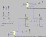
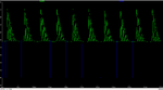
I'm trying to drive a H-bridge with 2 IR2110 drivers, but I have problems with the high side MOSFET gate drive. I'm using a 20kHz PWM drive. The circuit I'm testing is in attachment ("IR2110.txt"). On the file "Gate_voltage.png", there is the voltage on M1 gate (green), and the voltage on M3 gate (blue). The drive of the low side works well (M3) but as you can see on the green curve, the drive of the high side doesn't work.
I think I have an idea of where does the problem come from, but I would like to be sure. The control of the MOSFET that I want is :
- When I want to increase the current in the motor, VH1 and VL2 are high, so M1 and M3 are ON, and M2 and M4 are off. In my simulation, VH1 and VL2 are on for 10µs.
- Then there is the second part of the chopping, where the current decay through a recirculating path. With my control, all the MOSFET are off during this time. So the current is supposed to decay through the diodes D2 and D3, correct me if I'm wrong.
The problem with this control is that the bootstrap capacitor C2 of the IR2110 can never charge, because the control never bring the ground to the source of M1. So I'm assuming that's why my high side drive does not work properly. What do you think about that ? Is that the reason my circuit does not work ?
And now I would like to know : is there a way to get the IR2110 working with my kind of control ? I need to keep this control, because this is a requirement of my client...
Thank you,
Maxime.