Continue to Site

Welcome to EDAboard.com

Welcome to our site! EDAboard.com is an international Electronics Discussion Forum focused on EDA software, circuits, schematics, books, theory, papers, asic, pld, 8051, DSP, Network, RF, Analog Design, PCB, Service Manuals... and a whole lot more! To participate you need to register. Registration is free. Click here to register now.

GSM Power Amplifier Stability Issue

Status
Not open for further replies.

adnan012

Advanced Member level 1
Joined
Oct 6, 2006
Messages
468
Helped
2
Reputation
4
Reaction score
2
Trophy points
1,298
Activity points
4,923
Hi,

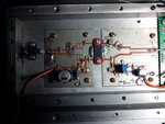
I have designed a GSM amplifier using MRFE6S9125N.The band width is 915 to 960 MHz . The out put power is 40 watts. I followed matching networks given in the datasheet on FR4. This amplifier is working well without any problem. It ' gain was set to 16 or17 db by using VNA. This amplifier is working well for months.

After this i tried to design the same amplifier for 880 to 915 MHz band with some changing in matching network capacitors value and location. I tested its gain on VNA and it was 18-19db (input power 0dbm from VAN ) at 24~28 volt dc and 600mA idq. I tested it at 40 to 65 watts power several times and the duration of each test was from 1 to 2 hour with antenna and with dummy load.

Today when i turned it on it showed no power on power meter .After debugging i found that gate was showing short to ground.

I want to ask few questions


1) After running it model in ADS LSSP with 30 dbm input power and with 50 ohm terminations it shows that the amplifier is not unconditionally stable at 10 MHz , and also from 280 to 450 MHz. However it is stable for the gsm band

Do i need to stabilize it at for the whole band?

2) What is the reason of amplifier damage? Some times only gate is damaged and some times both drain and gate are shorted to source

3) The input power is 30dbm. Can any power level above this damage amplifier?

4)Can i design amplifier at low gains say 15db by changing input and output matching networks? or only input matching network?
 

I think you should check this PA by terminating 50 Ohm its input and observe oscillations if there are with a SA.
Stability factors in simulations wouldn't say the reality in everytime.Unstabilities at higher frequencies should also be observed up to for instance 5GHz.
 
Your problem seems to may have two sources:

- a RF amplifier with unstable regions out of the desired band is prone to oscillation and this can kill it very fast. Oscillations of such kind often happen during switching on or of the DC power. You have to make sure this can never happen, e.g. by delaying the DC gate bias to "open" after the main DC voltage is applied, and switching off the gate voltage before switching off the main DC voltage.
- the RF input must be carefully filtered and limited before applying it to the wideband RF power amplifier. Any stray signal, out of band and above the maximum input power can cause problems. Overloading the amplifier by 2-3 dB can cause limiting but longer exposure will kill it. Again, input power and output SWR monitors must be used and well adjusted. If possible, use higher-power amplifiers to deliver a lower output. Test carefully the DC power supply and gate bias circuit: glitches do kill fast! Handle the temperature carefully, with spare fans, etc.
 
I am using switching power supply. I think it is generating glitches?

What is the proper method of biasing. i am using zener diode with potentiometer to adjust voltage for gate . Zener diode is powered directly from drain voltage.
Do i need to use separate power supplies for drain and gate ?
May i add large capacitor after the potentiometer wiper lege to add some delay.

I want to ask another question , MRF6v2150N is a vhf amplifier with 25 db gain at 220 MHz and 23 db at 450MHz according to datasheet.
Here is a comparison of input and output capacitance of both amplifiers MRFE6S9125N and MRF6v2150n.

MRF6v2150n MRFE6S9125N

input capacitance ------------------- 163pf 350Pf
output capacitance -------------- 93pf 63pf

MRF6v2150n simulation provide gain more than 15 db at 925MHz.

can i use it for 880 to 915 MHz with reduced gain?
 
Last edited:

I am using switching power supply. I think it is generating glitches?

What is the proper method of biasing. i am using zener diode with potentiometer to adjust voltage for gate . Zener diode is powered directly from drain voltage.
Do i need to use separate power supplies for drain and gate ?
May i add large capacitor after the potentiometer wiper lege to add some delay.

I want to ask another question , MRF6v2150N is a vhf amplifier with 25 db gain at 220 MHz and 23 db at 450MHz according to datasheet.
Here is a comparison of input and output capacitance of both amplifiers MRFE6S9125N and MRF6v2150n.

MRF6v2150n MRFE6S9125N

input capacitance ------------------- 163pf 350Pf
output capacitance -------------- 93pf 63pf

MRF6v2150n simulation provide gain more than 15 db at 925MHz.

can i use it for 880 to 915 MHz with reduced gain?

I think you can use the device if the gain is acceptable. I have indicated the problems above.
Most high-power amplifiers are prone to oscillation in or out of band and this must be treated to make the amplifier reliable.
The gate DC bias can be derived from the main DC power supply but please read again my text above. Protection and monitoring circuits must be well tested to make the amplifier reliable.

When one works with UHF amplifiers, a fuse to protect the device from an overcurrent must operate as fast as the UHF amplifier. One "wrong" cycle at UHF can kill the expensive amplifier and all care must be done to prevent it.
 
I am very thankful for you reply.

Can you please mention some text related Protection and monitoring circuits.
What type of fuse is used for this purpose?
 

With the UHF power amplifiers like yours, the switching on and off usually requires a procedure:

1. Before switching ON, reduce the RF input power switch or attenuator) and "close down" the gate bias.
2 THen slowly open the FET channel by gate bias while the output match monitor must indicate a good SWR.
3. If all is OK, then apply the full power input while the output SWR monitor must confirm the output match is OK.
4. Monitor the output SWR and temperature all the time of operation. Switch OFF whenever a problem is indicated.

5. When switching OFF, start with reducing or removing the input power.
6. By gate bias reduce channel current to a minimum.
7. Then reduce the main DC voltage.
8. Last switch off the cooling fan when the DC input is zero (no current).

- - - Updated - - -

I am in doubts that a good fuse (electronic) can be designed for the UHF amplifier. It would have to cut the current faster than within one nanosecond. Rather I recommend the procedure above.

It means no ON/OFF switch like a toggle to be used for the main power supply. The ON/OFF switch must trigger the timer to follow the procedure as above. You can use two or three 555 timers with relays to do it. If a trained person is to handle the switching ON/OFF procedure (assumed to occur once in a week or so), then train the person to follow it.

- - - Updated - - -

All the above problems make good UHF amplifiers an expensive device to buy. Reliability costs a good design work and a lot of testing before the release and sale.
 
Thanks

Before using MRFE6S9125N i worked on SD57060 AND BLF1046 . There amplifiers don't have internal ESD protection. At that time i was facing the same problem.

After setting the gain of there amplifiers on VNA. i connected the power amplifier to the driver stage, and most of the time, on power up they destroyed without any notice . I thought that it was due to ESD issue . Some amplifier at 50 watts worked for many days and then eventually destroyed. Can i conclude from this dissuasion that it was due to dc biasing issue not from ESD. If this is true , i can use SD57060 with the steps you mentioned above ?

I have also designed 1.8GH amplifer at 30 watts by using MRF6S18060N and never lost any device.

- - - Updated - - -

here is a picture of my 900 MHz amplifier which i designed few months ago . it is working well.
But i have to follow your recommendation for all my amplifiers.
 

Attachments

  • IMG_20130924_180240.jpg
    IMG_20130924_180240.jpg
    1.7 MB · Views: 142

Even MRFE6S9125N is mentioned in the datasheet that is designed for broadband applications, can be seen from the plots the performances are optimized for 920 MHz to 960 MHz frequency range, most probably using an internal match.
Would be an issue to tune for a lower frequency when an internal match is used.

MRF6S18060N is also optimized for 1.8 GHz, where you say that works fine.
 
I have two MRF6S18060N boards one from 1710 to 1780MHz and the second one from 1810 to 1880MHz.

MRFE6S9125N Data sheet shows that

GSM EDGE Application:
• Typical GSM EDGE Performance:

Pout= 60 Watts Avg., Full Frequency Band (865 - 960 MHz or 920 - 960 MHz)
 

Some amplifier devices are designed and optimized for specified bands, others can operate over a wide band. As I explained, even with a careful design any such amplifier can oscillate and kill itself very fast. The procedure I wrote makes sure the conditions for oscillation can be prevented.
 
thanks for reply .

I have started working on these steps.

May i assume that same issue killed my SD57060 AND BLF1046? At that time i thought that it was due to esd problem.

- - - Updated - - -

will inform you about the progress of sequencing hardware.
 

Status
Not open for further replies.

Part and Inventory Search

Welcome to EDABoard.com

Sponsor

Back
Top