Continue to Site

Welcome to EDAboard.com

Welcome to our site! EDAboard.com is an international Electronics Discussion Forum focused on EDA software, circuits, schematics, books, theory, papers, asic, pld, 8051, DSP, Network, RF, Analog Design, PCB, Service Manuals... and a whole lot more! To participate you need to register. Registration is free. Click here to register now.

Emitter Bias transistor operating principle

Status
Not open for further replies.

saviourm

Junior Member level 3
Joined
Apr 28, 2011
Messages
30
Helped
0
Reputation
0
Reaction score
0
Trophy points
1,286
Activity points
1,519
emitter bias.jpg
Dear Friends

First, thank you for your support and replies!
Currently I am studying the emitter bias config of a transistor please find fig attached. I have three questions in mind:
1 ,Why VCC doesn't effect the collector current and voltage drop across RE ?
2 Is this circuit is it like two supply emitter bias(the battery(VBB ) can be redrawn as the positive terminal faces to ground and negative terminal face the emitter resistor)?
3. This circuit can it be used as a current source?(please can you state the value of emitter resistor and the collector resistor for a current source)

Bst Wshs
SM
 

View attachment 96243
Dear Friends

First, thank you for your support and replies!
Currently I am studying the emitter bias config of a transistor please find fig attached. I have three questions in mind:
1 ,Why VCC doesn't effect the collector current and voltage drop across RE ?
2 Is this circuit is it like two supply emitter bias(the battery(VBB ) can be redrawn as the positive terminal faces to ground and negative terminal face the emitter resistor)?
3. This circuit can it be used as a current source?(please can you state the value of emitter resistor and the collector resistor for a current source)

Bst Wshs
SM
1. The voltage across RE is fixed at VBB - one junction drop across the BE junction. So VRE is VBB-0.6V
2. Not sure what you mean here.
3. The constant current source (or sink into the collector) is Iconst = (VBB - 0.6)/RE

In summary, the base voltage is fixed. The base emitter junction drops around 0.6V and makes the emitter voltage fixed.
This means the emitter current is set by RE.
As the Collector current is approx equal to the emitter current, then the current flow is independent of the VCC voltage
 
2, the VBB cant be reveresed If you do so the transistor will be switched OFF,

Ic = IE - IB // here IE and IB constant so the IC is also constant(when Vcc and Rc allows)....
 
I appreciate your reply, please can someone give me An operating principle of the circuit attached with real numbers.

Thanks
 

As an example if the base voltage was biased at +2V, then the emitter will be one diode drop (approx 0.6V) lower so will be at 1.4V

If RE is 1K then the current going throug RE is V/R = 1.4V/1k 1.4mA.

Now provided the collector has a resistor and supply voltage and the transistor is in its linear range, this same current will flow into the collector.
Assuming Vcc is 10V and RC is 1K, then the collector will be at Vcc - RCxIc. We have set Ic (=Ie) at 1.4mA as discussed so Vc will be at 10 - 1.4 = 8.6V

Even if Vcc drops to 8V the current through Rc will still be 1.4mA and Vc will drop to 8 - 1.4 = 6.6V

This constant current will work down to the point where Vc starts to approach Ve (plus a little for the transistor saturation).
So in this case allowing Vc down to 1.7V then VCC is 1.7 +1.4 = 3.1V

So here we have a constant current sink into the transistor collector that will work from a VCC 3.1V upwards.
Limits are the transistor breakdown voltages or thermal properties.

Errors are I am assuming the gain is high >100 such that Ib the current into the base can be ignored.
Also the transistor base emitter voltage assumed 0.6 is an approximation and varies with temperature.

Have a look at Proteus, I'm sure the free version will simulate a simple circuit, it just doesn't save or print, but that could help your understanding with near 'hands on' experience.

Hope this helps.
 
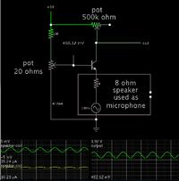
This resembles the common-base configuration, where the signal is applied at the emitter leg.

It is most useful when the incoming signal has low amplitude and low impedance.

Example, detecting signals in a wire coil.

Suppose we need a microphone, but all we have is a speaker. It is possible to turn a speaker into a microphone. The voice coil will produce AC at a small amplitude.

We need to add a pre-amp, to provide voltage gain. The common-base configuration is suitable. It can accept a signal at low input impedance. It has high voltage gain.


The output can be fed to a power stage (which provides current gain).

It was nice but we are talking about common emitter configuration.............

and also why 20 ohm pot in base side?
 

and also why 20 ohm pot in base side?

The pot is adjusted to create a stable fixed volt level at the base of the transistor.

The large gain is only obtained by applying around 0.4 to 0.6 V to the base. Proper positioning must be done by experimentation.

The lower the impedance, the better. The bias needs to be very stable, so it will not be thrown off by the low impedance signal at the emitter leg.

It was nice but we are talking about common emitter configuration.............

In that event, shouldn't the resistor be called an emitter feedback resistor? That is a typical method to obtain uniform gain when transistor characteristics are variable.

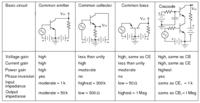
For my own part, I looked at the schematic in the initial post. And I thought, Which one of these transistor configurations is it closest to?


Furthermore, looking at the title of this thread, I gathered that the transistor is operated by applying the changing signal at the emitter leg. So that's the reason my simulation shows a common base amplifier.

However maybe this was incorrect on my part...

Because 'emitter bias' seems to require that the supply be bipolar, rather than single polarity (according to two or more of the links below).

http://en.wikipedia.org/wiki/Bipolar_transistor_biasing
(80 percent of the way down the page.)

http://www.learningaboutelectronics.com/Articles/Transistor-biasing-methods
(60 percent of the way down the page)

http://www.allaboutcircuits.com/vol_3/chpt_4/10.html
(many calculations shown at the above link)


After this I'm not sure which configuration to focus on.
 

Having re-read the original question "Currently I am studying the emitter bias config of a transistor", my answers are still approriate for understanding the circuit.

I think the previous post on the transistor configuration are correct, BUT the common "whatever" is something that you will discuss/learn next, i.e. the circuit shown is minimal and for understanding dc bias effects. The "common" part comes when you discuss amplification and have inputs and outputs. Just my thoughts......
 

The common-base configuration, where the signal is applied at the emitter source.

the base–emitter junction is forward biased, which means that the p-doped side of the junction is at a more positive potential than the n-doped side, and the base–collector junction is reverse biased. In an NPN transistor, when positive bias is applied to the base–emitter junction, the equilibrium is disturbed between the thermally generated carriers and the repelling electric field of the n-doped emitter depletion region. This allows thermally excited electrons to inject from the emitter into the base region. These electrons diffuse through the base from the region of high concentration near the emitter towards the region of low concentration near the collector. The electrons in the base are called minority carriers because the base is doped p-type, which makes holes the majority carrier in the base.

both the operations are switching transistor for further operation I’m not recommending but perhaps you could check out this **broken link removed**
 

Status
Not open for further replies.

Similar threads

Part and Inventory Search

Welcome to EDABoard.com

Sponsor

Back
Top