ghasem_008
Full Member level 4
Hi.
I'm familiar with FDTD very well.
I want to simulate a Photonic Crystal Fiber (PCF) using 2D FDTD.
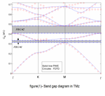
actually,I want to obtain following figure (figure 1).(this is a Band gap diagram).
in FDTD,we gain fields E and H.
How obtain this diagram from E,H fields?
y-axis is normalized frequency (a/λ).
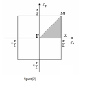
x_axis is vertices of a cell in PCF (see figure 2).

