el hou
Newbie level 4
Hi all,
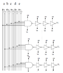
when I searched for a decoder design using in CMOS sensor I found the schematic shown in the picture , and this description : "The decoder used here is a simple NAND gate followed by 3 inverters for driving the row in the array (pixels matrix)."
I don't understand why he used three inverters !! And is it similar to use one inverter ?
when I searched for a decoder design using in CMOS sensor I found the schematic shown in the picture
 , and this description : "The decoder used here is a simple NAND gate followed by 3 inverters for driving the row in the array (pixels matrix)."
I don't understand why he used three inverters !! And is it similar to use one inverter ?