Continue to Site

Welcome to EDAboard.com

Welcome to our site! EDAboard.com is an international Electronics Discussion Forum focused on EDA software, circuits, schematics, books, theory, papers, asic, pld, 8051, DSP, Network, RF, Analog Design, PCB, Service Manuals... and a whole lot more! To participate you need to register. Registration is free. Click here to register now.

Problems,while creating layout in ADS 2009.

Status
Not open for further replies.

raju_kambar

Full Member level 3
Joined
Jun 19, 2013
Messages
153
Helped
5
Reputation
10
Reaction score
5
Trophy points
18
Location
Earth
Activity points
1,404
Dear Sir,

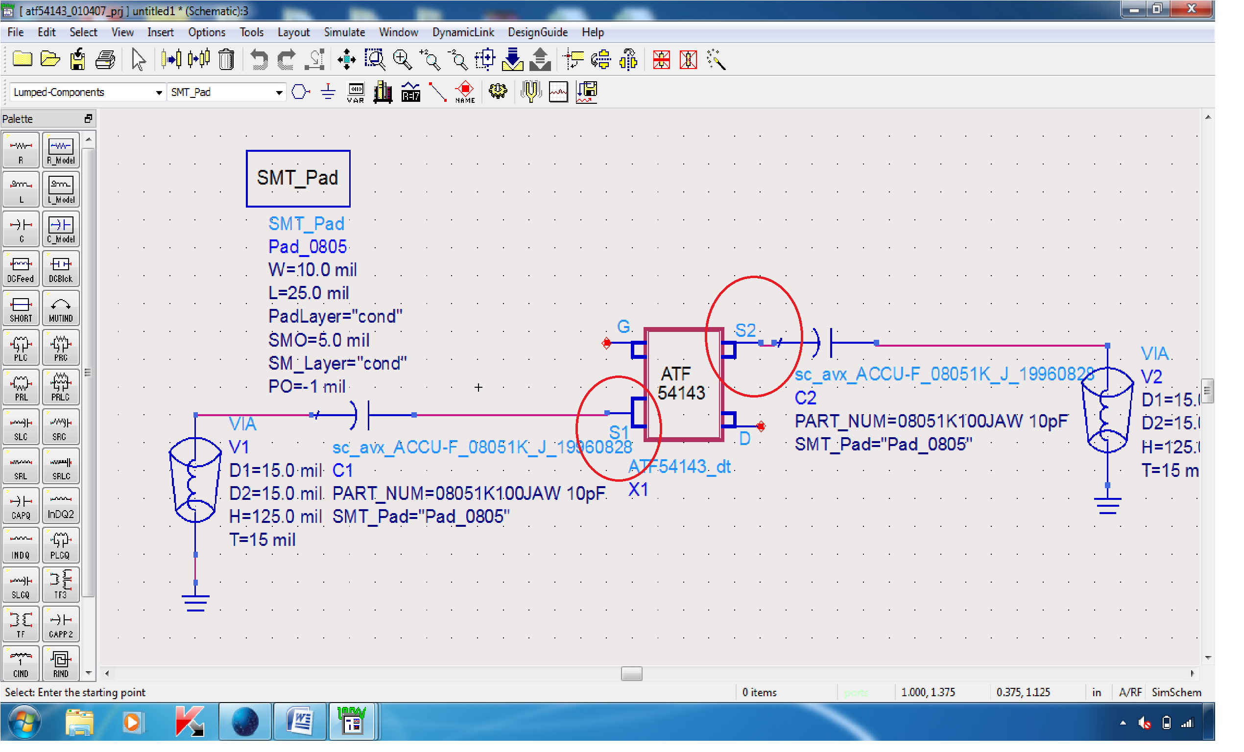
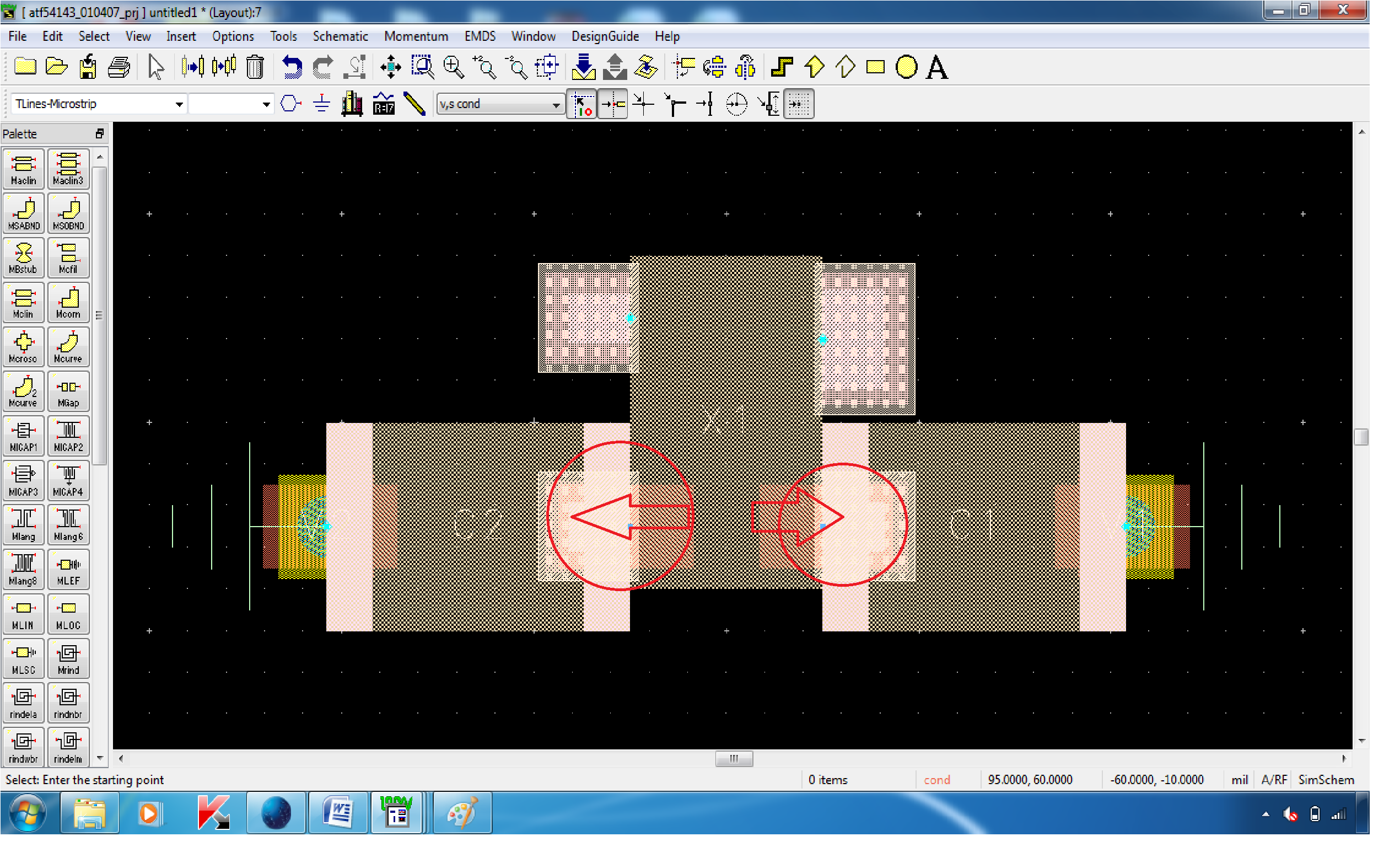
(1) I have taken ATF 54143 transistor. It is 4 pin IC , two sources are present diagonally opposite to each other. When I connected capacitors and VIAS two sides of the two sources of the ATF 54143 transistor and generated layout. In layout generation, ATF 54143 transistor layout generated, two sources are generating side by side. Sources are not generating diagonally opposite to each other, they are adjacent to each other in the layout generation. How to generate the ATF 54143 transistor two sources diagonally opposite to each other. One more thing physically transistors two sources are diagonally opposite to each other, if layout generation comes side by side two sources, while fabrication it is difficulty. I have shown below the images of Scheamtic_LAYOUT and Generated_layout.

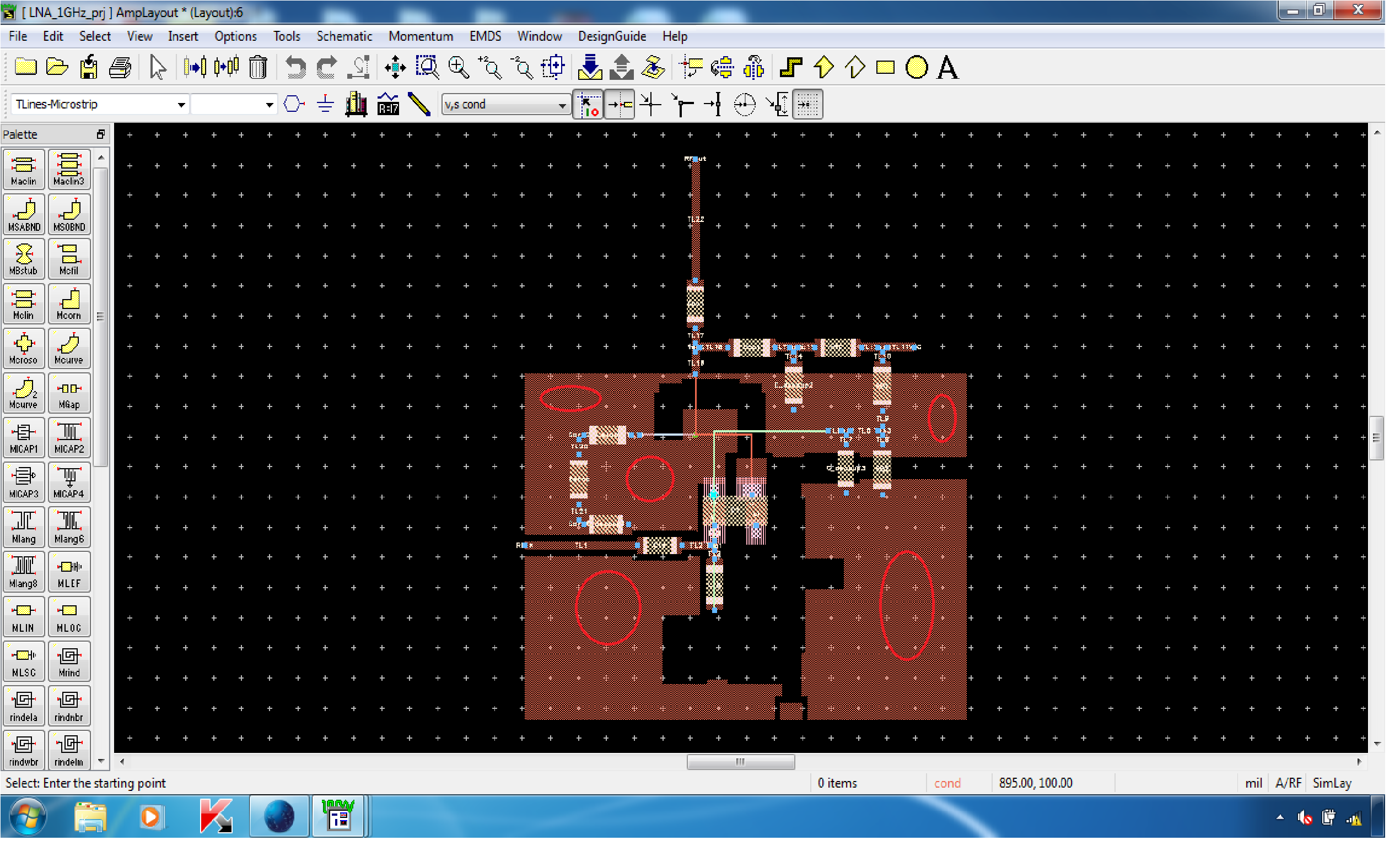
(2) One more difficulty, I have. I want to generate the two layers top layer and bottom layers in layout generation. I want to connect the VIA HOLE from top layer to bottom layer . How we can generate bottom and top layers in ADS 2009 and how we can connect the VIA HOLE from top to bottom layer through the substrate. I have noticed in the example from C:\ADS2009\examples\MW_Ckts\LNA_1GHz_prj, but they didn't use the VIA HOLE connection and bottom conductor. My question is , how to generate the top and bottom layers and connect the VIA HOLE from top to bottom through the substrate with some thickness , and also how to view the 3-dimesional view for top layer , bottom layer. Can you help me to sort out these difficulty.
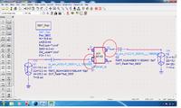
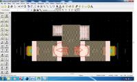
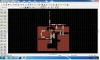


Dear Sir,
Can you any body help me to get the diagonal opposite sources in the generated layout as like in the schematic of ATF54143. I tried lot in the components settings of the ATF 54143 also, couldn't get it. Please help me to solve this correct generation of ATF terminals at both sides.
 

Did you created the footprint on yourself? Maybe you can adjust the pin mapping.
 
Did you created the footprint on yourself? Maybe you can adjust the pin mapping.
Johnjoe Sir,
Please help me, how to setting the pin mapping and how to get the footprint. My work has got struck there itself. Why ADS2009,it is generating like this. I don't know , how to setting the pin mapping and get the footprint. I request you to help me in this regard, it is also helpful to some other, who are facing the same type of problem using ATF54143. Please help me sir.

with best regards
raju.
 

Where did you got the footprint? Because I downloaded the model from avago and no footprint was included?
 
johnjoe Sir,
O.k.How can we adjust the pin mapping for the Avago ATF 54143 transistor for the proper generation of layout on either side in ADS2009. Can you explain me in detail.
 

Please reply to my question, where do you got the layout? Drawn on yourself? Because otherwise it's complicate to help.
 
johnjoe Sir,
I didn't draw the layout , have generated the layout from the custom model of ADS 54143 with capacitor and VIA using option in the schematic window Layout > Generate/Update. I have downloaded the .ZAP file of ADS MODEL of ATF54143 from AVAGO website. Later using the ADS 2009 , I unarchived the .ZAP. Then using component library , I got the 4 pin custom symbol of ATF 54143 and connected the SMT capacitor and VIA to the either side sources custom symbol of ATF54143. Later , I went to the Layout > Generate/Update Layout and generated the layout of custom model of ATF54143 with the connected component. Notice that I didn't adjust any pin mapping, even I don't know how to adjust the pin mapping.What ever I have shown in the posting #1 as like that layout generated with the side by side source not diagonally opposite.
 

Strange, because when I used the downloaded component, I've no layout component at all. I think easiest way is to draw your own footprint from datasheet. In the datasheet a footprint example is provided. Or maybe you can upload your project.
 
johnjoe Sir,
I am attaching .ZAP file of ATF54143 custom model with connected components. From this file only, I have generated the layout. I have created the ADS_ZAP_FILE_FOLDER.rar. In that folder, I have saved the desired .ZAP file. I request you to go through once and give me solution for correct pin generation of ATF54143 ADS model.
 

Attachments

  • ADS_ZAP_FILE_FOLDER.rar
    36.9 KB · Views: 59

Dear raju_kambar,

i found the mistake, (there are two). First, if you compare datasheet and schematic symbol, you'll find that the big source pin is not next to gate, but next to drain. But it's not the problem. Second, somebody assigned a standard SOT343 footprint to the schematic symbol. If you flatten your layout and push into the footprint of your transistor, a standard sot343 layout will open. There you see small red lines, these are the pin assignments. Change their numbers, save it as new layout and assign it to your schematic symbol. Finished :)!
 
johnjoe Sir,
Thank you for your priceless help,it helped me like anything. I am really thankful to you. I only assigned SOT 343 fixed art work for the ADS custom symbol model to generate the artwork for the ATF54143 ADS model( because ready made layout model was not available for the ATF 54143)." If you flatten your layout and push into the footprint of your transistor, a standard sot343 layout will open. There you see small red lines, these are the pin assignments. Change their numbers, save it as new layout and assign it to your schematic symbol. Finished".. I am confused little, what I have to do . Can you show me graphically , what I have to do for getting correct layout generation. How we open the standard sot343 layout. Please don't mine, can show me graphically. I am sorry.
 

No problem, but I'll post it in 4-5 hours. I'm little bit busy.
 
johnjoe Sir,
O.k. thank you sir, don't forget it.

- - - Updated - - -

johnjoe Sir,
As you said, I followed . Now it is coming nicely , now layout is generating nicely as like the schematic. I did as you said, changed the SOT343 pin numbers and changed. I am really grateful to your priceless help. Thank you... thank you very much for your help. I am very much satisfied with patience help. Thank you, if any problem comes in this regard, I will ask you sir.
 

Status
Not open for further replies.

Part and Inventory Search

Welcome to EDABoard.com

Sponsor

Back
Top