Welcome to our site! EDAboard.com is an international Electronics Discussion Forum focused on EDA software, circuits, schematics, books, theory, papers, asic, pld, 8051, DSP, Network, RF, Analog Design, PCB, Service Manuals... and a whole lot more! To participate you need to register. Registration is free. Click here to register now.
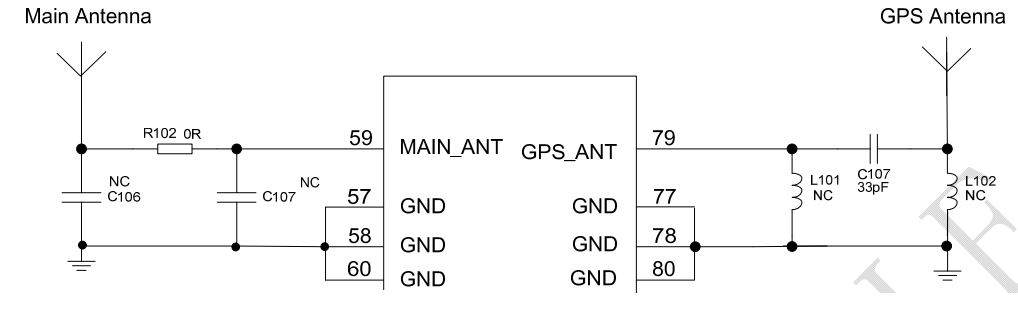
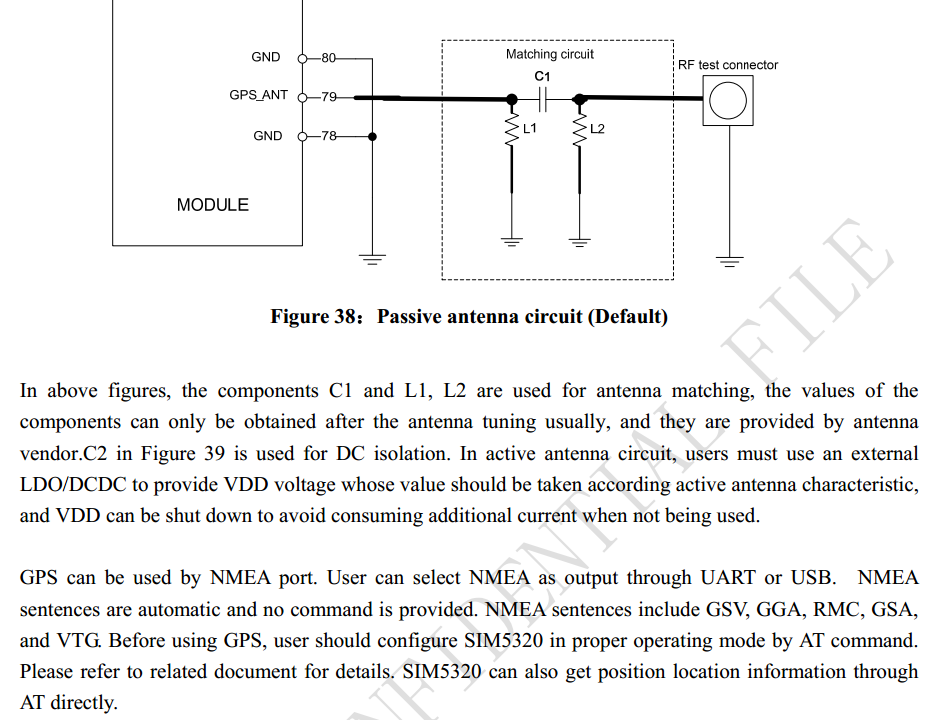
As described in attached pictures, these components are used for antenna matching.
Now antenna matching is "To match the impedance of Module's ANT pad to 1. PCB trace from ANT-pad to antenna & 2. antenna itself."
Usually, impedance of antenna is 50 ohm and impedance of Module's ANT pad is also 50 ohm. so in order to match the impedance you need to route a 50 ohm trace from Module's ANT pad/pin to antenna.
The values of matching circuit are decided only "after" PCB fabrication. when PCB is ready, you measure the impedance of ANT-to-antenna trace and if it's not 50 ohm, you adjust the values of these components to make it 50 ohm.
Google characteristic impedance and controlled impedance routing.
and if you don't have access to a Vector Network Analyzer to measure the impedance, just remove all of these components and simply route an impedance-controlled-trace(microstrip, stripline or coplanar waveguide) from ANT pad to antenna connector. This solution is not ideal but works
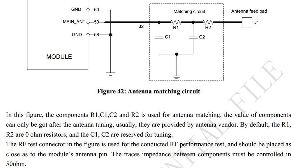
This site uses cookies to help personalise content, tailor your experience and to keep you logged in if you register.
By continuing to use this site, you are consenting to our use of cookies.
")