Continue to Site

Welcome to EDAboard.com

Welcome to our site! EDAboard.com is an international Electronics Discussion Forum focused on EDA software, circuits, schematics, books, theory, papers, asic, pld, 8051, DSP, Network, RF, Analog Design, PCB, Service Manuals... and a whole lot more! To participate you need to register. Registration is free. Click here to register now.

[MOVED] Help with simulating inverter

Status
Not open for further replies.

wakeup12

Newbie level 3
Joined
Aug 13, 2013
Messages
3
Helped
0
Reputation
0
Reaction score
0
Trophy points
1
Activity points
24
Hello,

I just registered for the forum and have a problem with my first layout design. I am trying to design layout, schematic and symbol, and then using symbol or schematic to test my design.

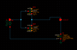
Here is the schematic:

sign_internals5.png

And here is the layout I designed:


sign_internals3.png

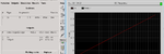
When I run DRC, I get the following warnings:

sign_internals2.png

Why does it still say that I have "not stamped connections"?
 

Attachments

  • sign_internals1.png
    sign_internals1.png
    7.6 KB · Views: 81
  • sign_internals4.png
    sign_internals4.png
    17.6 KB · Views: 84
Last edited:

I have never gotten that DRC message as far as I can remember, but perhaps if you fix the fundamental errors in your layout the message might dissappear.

1. Change the supply contacts(just interchange the ones you have). Ntap for VDD and Ptap for GND. (You have the opposite i your attachment.)
2. I cant see that you have a nwell. Add them to the pmos transistor. Make sure that the same nwell surrounds both the Pmos and the ntap substrate contact.
3. Add lables at inputs/outputs/supplies.
4. Search the web for layout tutorials. There are alot of them explaining what you are trying to do.
 

Thanks for answer,

1. I have Pmos at the bottom (yellow) and Nmos at the top, do I still need to change?
2. You mean ntub? Again the rectangle box (with X error) around pmos and ptap is NTUB. I am using Virtuoso Layout Editor version 5.10 and could not find NWELL in LSW.
3. I have them, but it hides them at each startup.
4. Thanks I will try for the future designs.

- - - Updated - - -

which simulator are you using?

How can I find out?
 

Usually people put PMOS on top and NMOS on bottom, but in makes no difference. You do your layout how you feel it should be made.

Yes Nwell and Ntub are the same thing.

I did not mean that you should change the transistors. I meant that you should change the substrate contacts.

In Virtuoso, I think the default shortcut for placing contacts is "o". Place "PD_C" close to the NMOS and "ND_C" close to the PMOS (The "ND_C" should be inside the NTUB of the PMOS in order to supply the voltage to the PMOS body)

You can find out what simulator you are using in Analog Design Environement -> Setup -> Simulator/Directory/Host ...

Just a question, it looks like you draw your transistors manually or?
 

connect pmos in pull up section and nmos in pull down section.while pmos source is connected to Vdd and nmos source is connected to ground.
 

Status
Not open for further replies.

Part and Inventory Search

Welcome to EDABoard.com

Sponsor

Back
Top