Continue to Site

Welcome to EDAboard.com

Welcome to our site! EDAboard.com is an international Electronics Discussion Forum focused on EDA software, circuits, schematics, books, theory, papers, asic, pld, 8051, DSP, Network, RF, Analog Design, PCB, Service Manuals... and a whole lot more! To participate you need to register. Registration is free. Click here to register now.

CPW EXcitation porblem

Status
Not open for further replies.

khubu

Newbie level 4
Joined
Aug 9, 2013
Messages
7
Helped
0
Reputation
0
Reaction score
0
Trophy points
1
Activity points
55
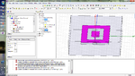
Would please anybody complete this patch antenna that i have attached...!! I Am confused on how to excite a Coplanar waveguide fed.. and which solution setup would be applied Driven model or driven terminal, I read the Help section ... but technical terms is hard to understand. Moreover, I am new to HFSS, considering a Good tutorial on CPW fed will be of great help...! I just need a finishing touch to my project.

please help me out.. because of this I am stuck in other projects too.
 

Attachments

  • slot_patch.rar
    10.4 KB · Views: 58

I have made a Slot patch antenna with square slot.. with CPW fed, the ground plane are on either sides of the signal/patch..! i have some quires:
- how to differ between a signal/patch and ground since both are assigned boundary signal/patch=perfectE , Ground=finiteconductivity, The differ i am asking is according to excitation to signal/patch via transmission line.

I have used edge lumped port (that is at the end of the transmission line) and solution type as a Driven terminal... the error i am getting is " [error] Port refinement, process hf3d error: Too few conductors were found on port 2. There should be one conductor for each terminal, with one additional reference conductor. Unintentional contact between conductors may cause this error.. (6:47:04 AM Aug 11, 2013)
[error] hfsscomengine, process hf3d died unexpectedly. (6:47:04 AM Aug 11, 2013)
[error] Simulation completed with execution error on server: Local Machine. (6:47:04 AM Aug 11, 2013)"


Please find me a solution regarding conditions to accommodate ground plane on topside of the substrate and excitation to cpw.. moreover, how to tell the software (hfss) the difference between signal/patch and ground... since port is common to signal/patch and ground

SEE THE PICTURE.. the GND and Patch/signal is been highlighted.
 

Attachments

  • problmepa.png
    problmepa.png
    224.5 KB · Views: 83

Hi Khubu,
I am working on Coplanar waveguide and i am also facing the same problem of Port exitation. My cut off frequency is 1.9 GHz. I exited coplanar waveguide with Waveport and i am getting 1.8 GHz. My question is Is that correct or else is der any other way to exite the Coplanr waveguide
 

Status
Not open for further replies.

Part and Inventory Search

Welcome to EDABoard.com

Sponsor

Back
Top