T3STY
Full Member level 4
Hello everybody!
As many of you helped me on making the circuit of this project I really want to thank you all! I could probably never make this on my own!
This project has been used during my graduation exams at high school just a few days ago (July 2nd, 2013) and teachers had no words for it!
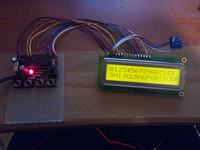
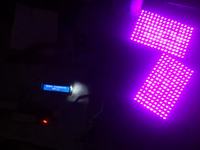
Here's the preview of the final product:
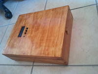

This being said, what's LED.EX?
LED.EX is an UV exposure tool that allows creating circuits (PCB) by using UV rays. The difference between my project and many others you'll find on the web is that mine uses UV LEDs instead of UV neon lamps, and, the most important part of it, it has a control board that counts the exposure time and allows to store it for further usage!
It works with special copper boards that use a light mask to impress the circuit traces. Once exposed to UV it can be immersed into acid to cut out the extra copper; only the part of copper exposed to UV light will be cut out, leaving the circuit traces behind.
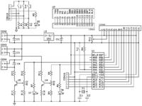
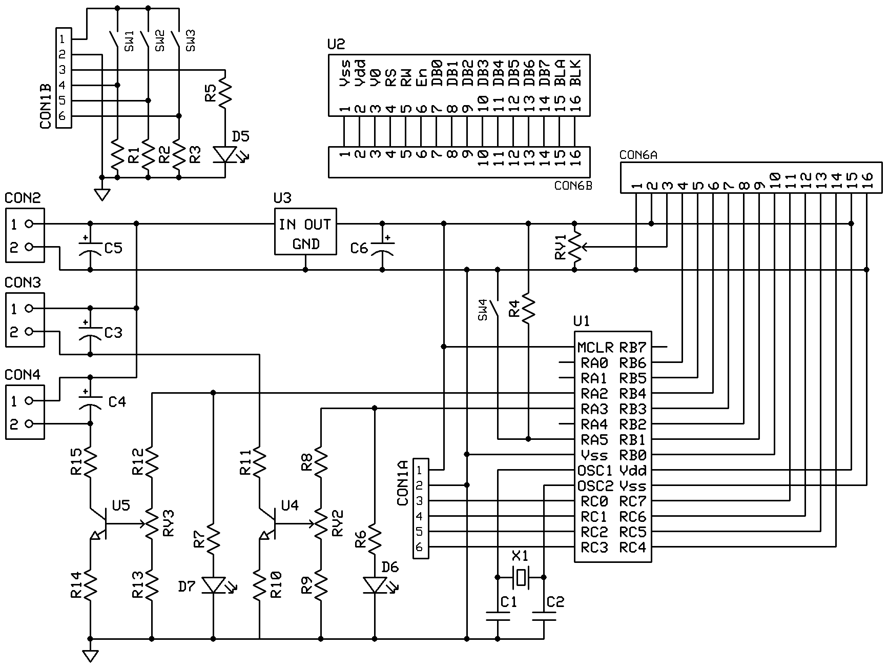
Next there is the electric schematic. It's very simple so many could build it on their own even on a breadboard.
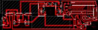
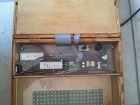
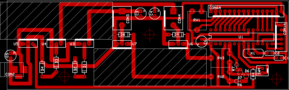
This is the main control board, and the PCB picture. Please note the schematic is newer while the PCB is from an earlier version of the circuit where I was having two 7812 voltage regulators (U3 and U4) and 4 diodes (1N4007) for rising the voltage up to 13.4V. In the final project I took out these parts and short-circuited the input and output pins of them, so all the power is tied directly to the transistors.
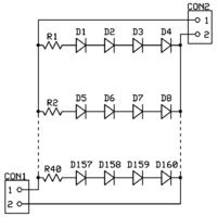
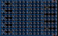
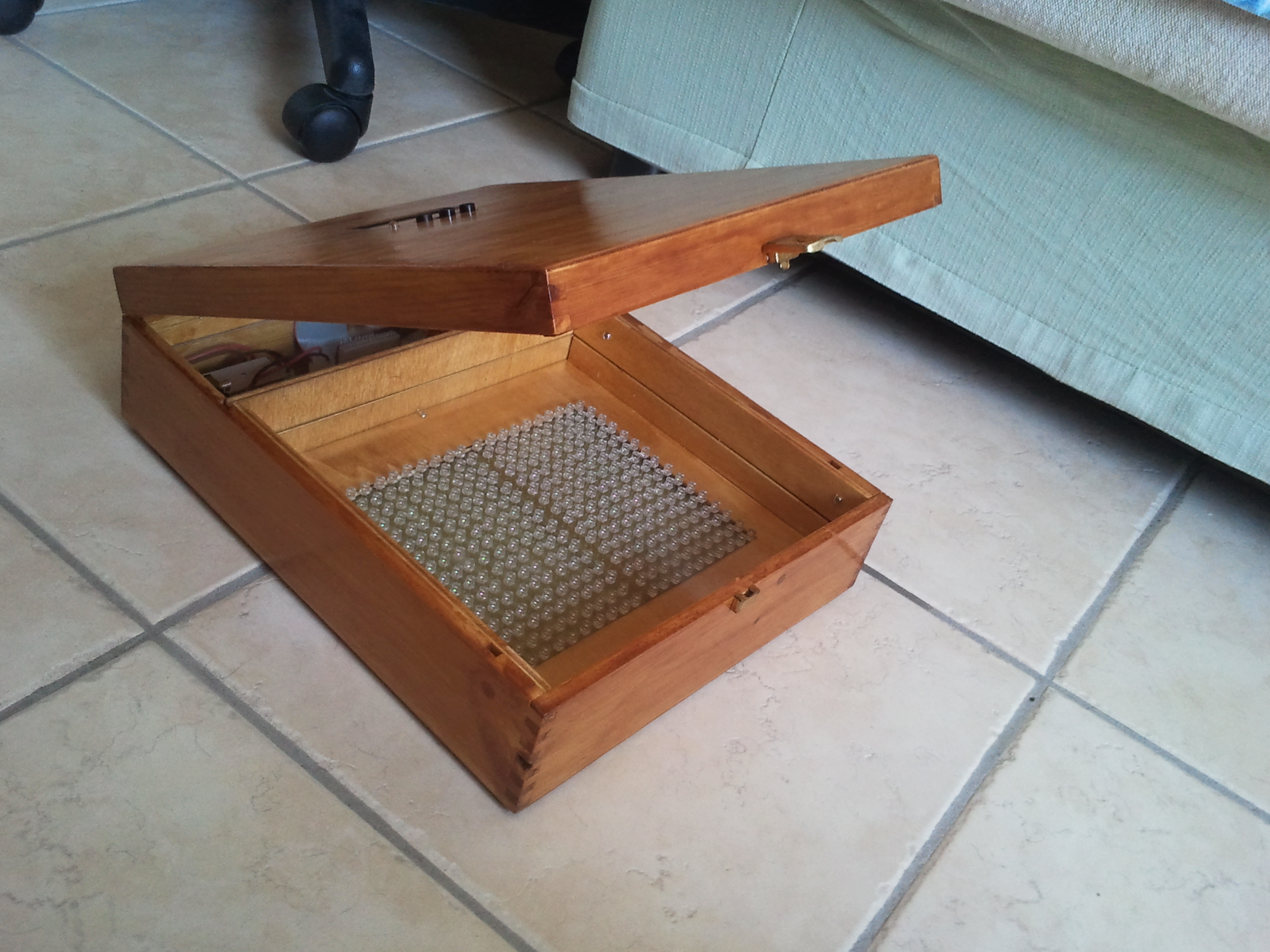
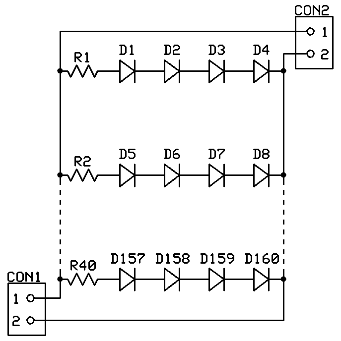
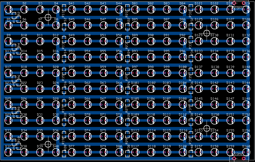
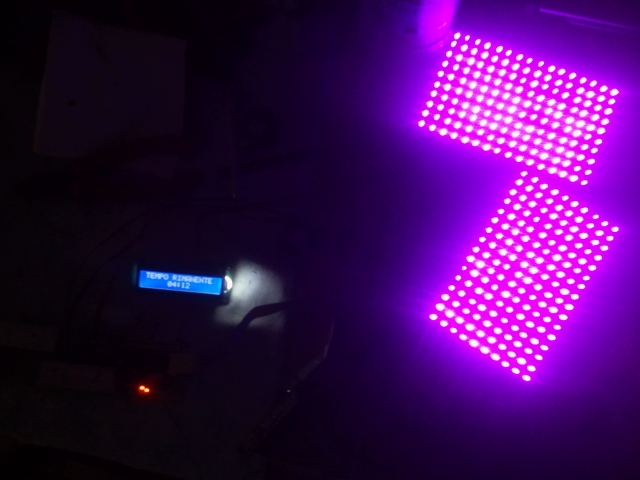
This is the LED board and the PCB picture. The two connectors on the sides are meant for power supply. in the PCB, LEDs are placed in a regular 16x10 grid and each LED is 1cm far from all others. That's very high density and ensures that the UV light does not lack any portion of the board. The resistors used are SMD in the 0804 package.
...and the components list:
Attached to this page there is a zip file containing the MPLAB project for PIC16F876. The source code of the project is written in C and has to be compiled with Hi-Tech's C compiler (works fine both Pro and Lite version).
The circuits provided can work with a variety of DC power supplies, starting from 5V up to 30V (just make sure it can carry out the total load).
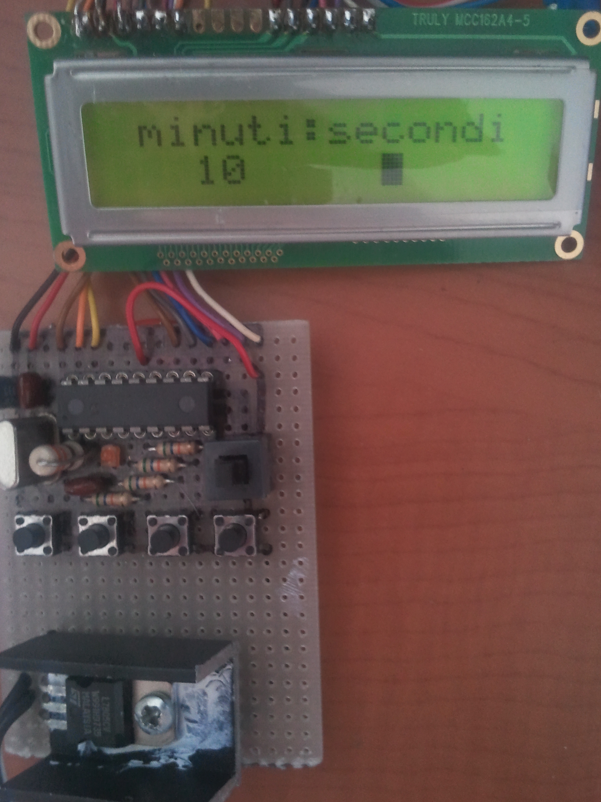
The main board has a 7805 voltage regulator that will power the PIC and the LCD display, and the 4 switches. SW1, SW2 and SW3 use the R1, R2 and R3 pull-up resistors, and they are needed to interact with the software on the PIC. SW4 is a saftey switch: UV rays are dangerous, is better not to be hit by them if you accidentally open the top panel.
The LED boards are powered through the 2 NPN transistors. The transistors I have chosen (2SC4793) are set to power the load (LEDs) on the collector, and they have high hfe (min 100, max 350) so they're perfect for driving even huge loads directly with the low current output of the PIC (about 25mA max).
The main board has been made to control 2 spearate LED boards. Each LED board uses in parallel many series of LEDs. You may put up to 9 LEDs in series with a maximum power supply of 30V. In the final project the power supply I have chosen is a 13.5V switching power supply (already made) and I have built 2 LED boards of 160 LEDs each (4 LEDs in series, 40 series for each board), with 68 Ohm resistor for each series (around 15mA max per series) for a total current of 600mA per board (8W). The transistors though have a potentiometer (RV2, RV3) that it's used to control the maximum brightness of the LEDs. Whatever the power supply you'll be using, and whatever the load is, make sure the LEDs are not too bright.
In the project the 2 LED boards I made have been positioned to extend the maximum circuit size to 20x16 cm. Also, the LEDs used in the final project are flat-top with 120° light angle (best light between 30° and 90°); and the exposing circuit is placed on a glass surface at 2cm height up of the LEDs. This ensures that UV light coming from the LED boards is totally uniform and it helps when the acid cuts out the extra copper because there won't be areas where the process takes longer than others. If you'll be making this project try not to use round-top LEDs because they have a center light beam with very restricted covering area, and this will produce a "dotted-blur" exposure.
About the software, I just finished it a few days ago and I'm unable at the time of writing to translate (most of it is Italian) and comment the code. Moreover, the software is very rudely implemented, not optimized at all. Still.. it works . I'm planning to rewrite it from scratch; if so I'll be updating you here.
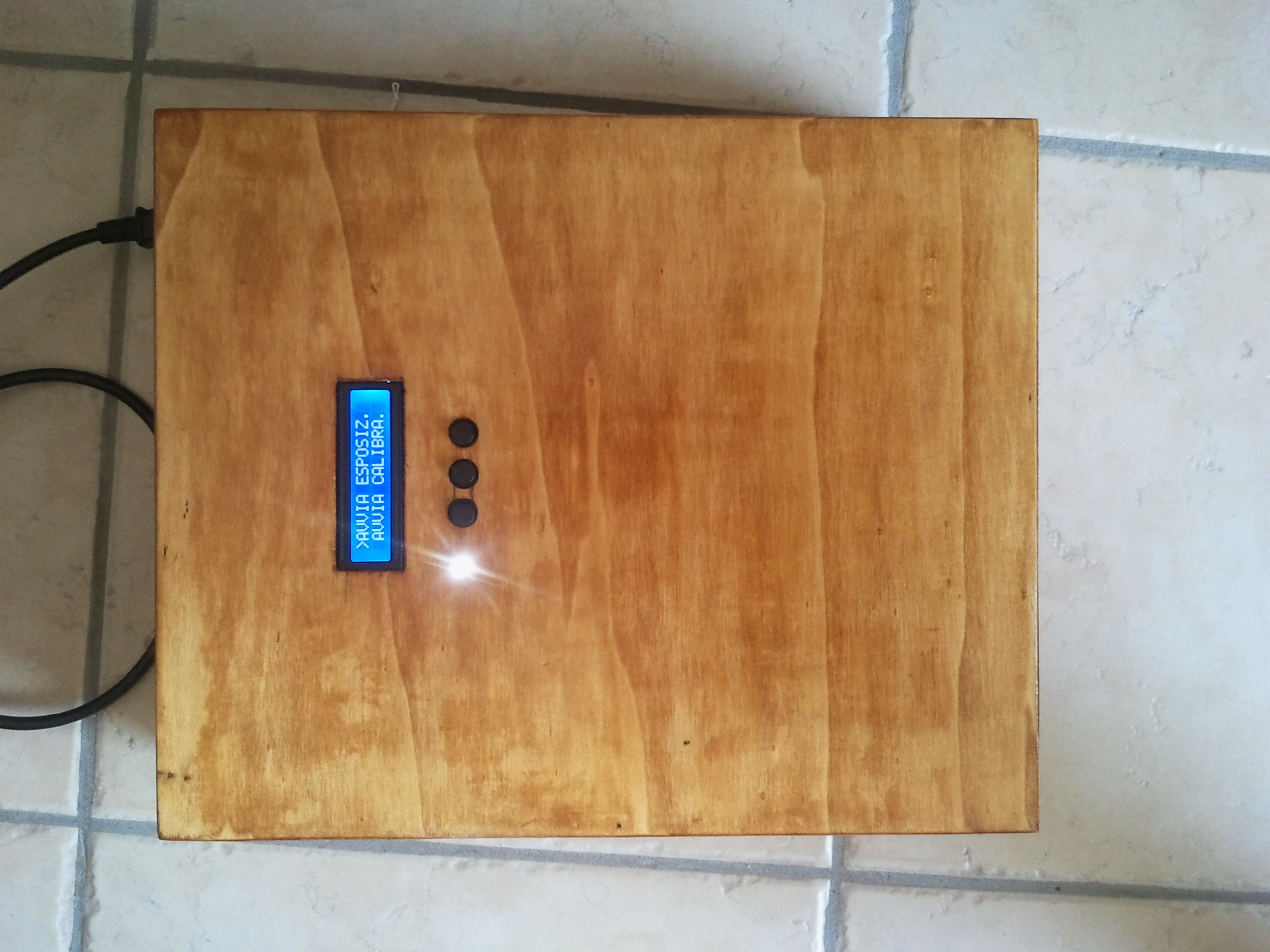
A very short help guide: there are only 3 buttons used in the project: UP, DOWN, ENTER. I guess there is not much need to explain what each does... anyway, use UP/DOWN to select a menu item, increase/decrease values or to select a message answer (some interactive messages on the display have "S/N" at the end, which is a simple Yes/No dialog - the choice blinks) and then press Enter to confirm.
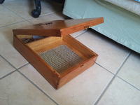
Before I leave you I'll post some more images of the project (even early development). Unfortunately, I don't have the right copper boards to show a demo of the project in action, but I'll soon make one!
An early stage development breadboard prototype.... it scares me everytime I look at it!

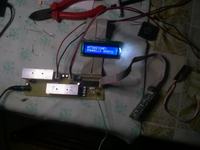
The PCB actually used in the final project during the testing.
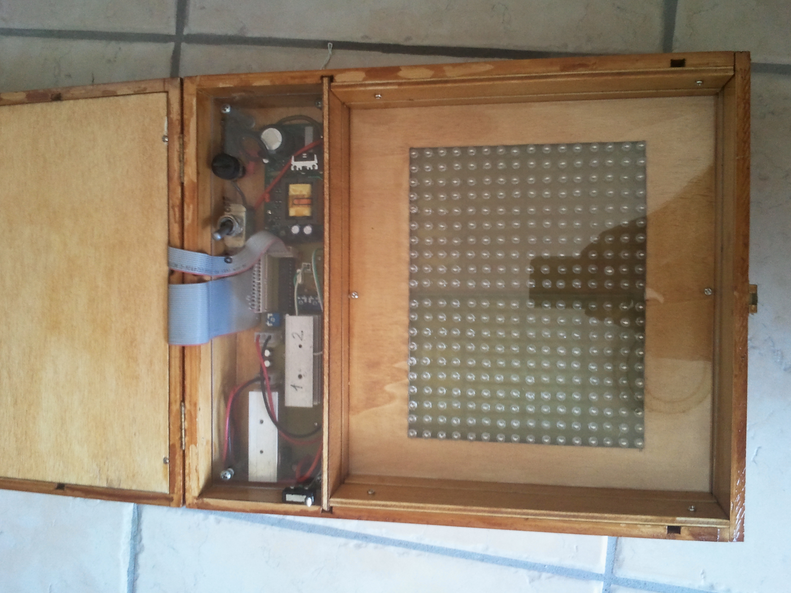
And a closer look to how it's made. For your interest, the box contained 3 bottles of wine... they magically disappeared to make room for anything else

That's all folks! I hope you'll enjoy this work as much as I do. Should you have any questions about it, or if you make a porting of the software for other compilers/PICs, just contact me!
LICENSE
The whole work is released under GPL version 3 License. Make sure you read the file License.txt included in the archive or read it online here:
https://www.gnu.org/licenses/gpl.txt
DISCLAIMER
As many of you helped me on making the circuit of this project I really want to thank you all! I could probably never make this on my own!
This project has been used during my graduation exams at high school just a few days ago (July 2nd, 2013) and teachers had no words for it!
Here's the preview of the final product:

This being said, what's LED.EX?
LED.EX is an UV exposure tool that allows creating circuits (PCB) by using UV rays. The difference between my project and many others you'll find on the web is that mine uses UV LEDs instead of UV neon lamps, and, the most important part of it, it has a control board that counts the exposure time and allows to store it for further usage!
It works with special copper boards that use a light mask to impress the circuit traces. Once exposed to UV it can be immersed into acid to cut out the extra copper; only the part of copper exposed to UV light will be cut out, leaving the circuit traces behind.
Next there is the electric schematic. It's very simple so many could build it on their own even on a breadboard.
This is the main control board, and the PCB picture. Please note the schematic is newer while the PCB is from an earlier version of the circuit where I was having two 7812 voltage regulators (U3 and U4) and 4 diodes (1N4007) for rising the voltage up to 13.4V. In the final project I took out these parts and short-circuited the input and output pins of them, so all the power is tied directly to the transistors.
This is the LED board and the PCB picture. The two connectors on the sides are meant for power supply. in the PCB, LEDs are placed in a regular 16x10 grid and each LED is 1cm far from all others. That's very high density and ensures that the UV light does not lack any portion of the board. The resistors used are SMD in the 0804 package.
...and the components list:
Code:
** MAIN BOARD **

[CONNECTORS]
CON1A+CON1B: 6 pin M+F connector
CON2, CON3, CON4: 2 pin, M, high power connector
CON6A+CON6B: 16 pin M+F connector

[ICs]
U1: PIC16F876(A)
U2: LCD display, 16x2, HD44780 controller
U3: 7805 - 5V fixed voltage regulator
U4, U5: 2SC4793 - high hfe (min: 100) NPN transistor

[SWITCH]
SW1, Sw2, SW3, SW4: simple button switch

[RESISTORS]
VR1: from 1K to 10K LIN potentiometer
    it controls the LCD backlight brightness
VR2, VR3: 2.2K LIN potentiometer
R1, R2, R3, R4: 1K, 0.25W
R5, R6, R7: 330 Ohm, 0.5W
R8, R9, R12, R13: 100 Ohm, 0.25W
(optional) R10, R14: any
    needed if the transistor heats up
    because of high voltage on Emitter
(optional) R11, R15: any
    needed if the voltage on collector
    is over the supported collector
    voltage of the transistor

[CAPCITORS]
C1, C2: non-polarized, any from 15pF to 30pF
(optional) C3, C4, C5: polarized, electrolytic, from 10uF up to 47uF, 50V
    these are power filtering capacitors
C6: polarized, electrolytic, 10uF, 16V
    to be placed the nearest to the PIC

[All other]
X1: 4MHz crystal oscillator
D5, D6, D7: LED diodes, rating 3V @30mA

** LED BOARD **
all resistors should be calibrated for 15 to 20 mA.
LEDs are UV-A emitting diodes, flat-top, rated for 3V@30mA.
Attached to this page there is a zip file containing the MPLAB project for PIC16F876. The source code of the project is written in C and has to be compiled with Hi-Tech's C compiler (works fine both Pro and Lite version).
The circuits provided can work with a variety of DC power supplies, starting from 5V up to 30V (just make sure it can carry out the total load).
The main board has a 7805 voltage regulator that will power the PIC and the LCD display, and the 4 switches. SW1, SW2 and SW3 use the R1, R2 and R3 pull-up resistors, and they are needed to interact with the software on the PIC. SW4 is a saftey switch: UV rays are dangerous, is better not to be hit by them if you accidentally open the top panel.
The LED boards are powered through the 2 NPN transistors. The transistors I have chosen (2SC4793) are set to power the load (LEDs) on the collector, and they have high hfe (min 100, max 350) so they're perfect for driving even huge loads directly with the low current output of the PIC (about 25mA max).
The main board has been made to control 2 spearate LED boards. Each LED board uses in parallel many series of LEDs. You may put up to 9 LEDs in series with a maximum power supply of 30V. In the final project the power supply I have chosen is a 13.5V switching power supply (already made) and I have built 2 LED boards of 160 LEDs each (4 LEDs in series, 40 series for each board), with 68 Ohm resistor for each series (around 15mA max per series) for a total current of 600mA per board (8W). The transistors though have a potentiometer (RV2, RV3) that it's used to control the maximum brightness of the LEDs. Whatever the power supply you'll be using, and whatever the load is, make sure the LEDs are not too bright.
In the project the 2 LED boards I made have been positioned to extend the maximum circuit size to 20x16 cm. Also, the LEDs used in the final project are flat-top with 120° light angle (best light between 30° and 90°); and the exposing circuit is placed on a glass surface at 2cm height up of the LEDs. This ensures that UV light coming from the LED boards is totally uniform and it helps when the acid cuts out the extra copper because there won't be areas where the process takes longer than others. If you'll be making this project try not to use round-top LEDs because they have a center light beam with very restricted covering area, and this will produce a "dotted-blur" exposure.
About the software, I just finished it a few days ago and I'm unable at the time of writing to translate (most of it is Italian) and comment the code. Moreover, the software is very rudely implemented, not optimized at all. Still.. it works
. I'm planning to rewrite it from scratch; if so I'll be updating you here.A very short help guide: there are only 3 buttons used in the project: UP, DOWN, ENTER. I guess there is not much need to explain what each does... anyway, use UP/DOWN to select a menu item, increase/decrease values or to select a message answer (some interactive messages on the display have "S/N" at the end, which is a simple Yes/No dialog - the choice blinks) and then press Enter to confirm.
Before I leave you I'll post some more images of the project (even early development). Unfortunately, I don't have the right copper boards to show a demo of the project in action, but I'll soon make one!
An early stage development breadboard prototype.... it scares me everytime I look at it!

The PCB actually used in the final project during the testing.

And a closer look to how it's made. For your interest, the box contained 3 bottles of wine... they magically disappeared to make room for anything else

That's all folks! I hope you'll enjoy this work as much as I do. Should you have any questions about it, or if you make a porting of the software for other compilers/PICs, just contact me!
LICENSE
The whole work is released under GPL version 3 License. Make sure you read the file License.txt included in the archive or read it online here:
https://www.gnu.org/licenses/gpl.txt
DISCLAIMER
Code:
This program is free software: you can redistribute it and/or modify it under the terms of the GNU General Public License as published by the Free Software Foundation, either version 3 of the License, or (at your option) any later version.

This program is distributed in the hope that it will be useful, but WITHOUT ANY WARRANTY; without even the implied warranty of MERCHANTABILITY or FITNESS FOR A PARTICULAR PURPOSE. See the GNU General Public License for more details.
Attachments
Last edited: