Continue to Site

Welcome to EDAboard.com

Welcome to our site! EDAboard.com is an international Electronics Discussion Forum focused on EDA software, circuits, schematics, books, theory, papers, asic, pld, 8051, DSP, Network, RF, Analog Design, PCB, Service Manuals... and a whole lot more! To participate you need to register. Registration is free. Click here to register now.

Problem with layout of Gain Boosting Op_Amp

Status
Not open for further replies.

hardyboy_86

Junior Member level 2
Joined
Apr 13, 2011
Messages
21
Helped
0
Reputation
0
Reaction score
0
Trophy points
1,281
Activity points
1,433
Hi,

I have Layout the design of Gain Boosting Op_Amp but i am experiencing a major issue in post layout that its Unity Gain frequency is going below half of the total,
My gain boosting op_amp is designed for 1.3 GHZ with 77 Degree phase, but in post layout after every effort i managed to get it to 904 MHZ with 65 Degree of phase,,

Plz Let me know what steps should i take to resolve this issue.

Thanks Alot!!
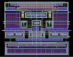
 

It's quite normal that UGF and PM of the layout implementation of RF circuits decrease a lot compared to the schematic. But without showing your current layout you can't get any help here, I'm afraid.
 
2.JPGCapture123.JPG


This is the layout design of Gain Boosting Op_Amp,,
 

Your layouts seem quite good, I think. You could try and analyze the parasitics from the extracted netlist (PEX) and see where you perhaps could decrease them - e.g. by larger distances. Otherwise you'll have to accept a 33% UGF decrease from schematic to layout, I'm afraid. Probably you'll have to develop a ≈2GHz schematic amp to reach the required bandwidth in layout. May be this involves the usage of a process with smaller geometries.
 
Try to resimulate your opamp with "rf" transistors - they including some additional capacitances and are more accurate.
 
Dear erikl
i have already lower the values of output capacitors and got unity gain frequency around ~1.6 GHz with 58 Degree of phase in pre layout, and after re modifying the output path in layout the post layout results are changed to 950 MHz with 65 Degree of phase.
Can you suggest some more tips to increase it more.

Dear Dominik Przyborowski

I'll consider you suggestion and it would be better to use rf transistors if no other method would work.
 

Can you suggest some more tips to increase it more.
  • In schematics, use Dominik's suggestion to simulate with more realistic parasitics.
  • From the extracted layout first check your PEX values and find out which of them contribute most to the UGF decrease.
  • Use smaller W/L ratios, and in any case minimum L .
  • More distance between transistors and guardRing.
 
Dear erikl

Thank You so much for your suggestions , I'll try your suggestions and let you know about the results.

Thanks Alot
 

Status
Not open for further replies.

Part and Inventory Search

Welcome to EDABoard.com

Sponsor

Back
Top