Continue to Site

Welcome to EDAboard.com

Welcome to our site! EDAboard.com is an international Electronics Discussion Forum focused on EDA software, circuits, schematics, books, theory, papers, asic, pld, 8051, DSP, Network, RF, Analog Design, PCB, Service Manuals... and a whole lot more! To participate you need to register. Registration is free. Click here to register now.

Synchronous boost converter floating transistor question

Status
Not open for further replies.

mavrik2k

Newbie level 6
Joined
Jul 24, 2009
Messages
14
Helped
0
Reputation
0
Reaction score
0
Trophy points
1,281
Location
Netherlands
Activity points
1,377
Hi every one ,
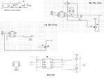
I want to design a synchronous boost converter upto 60 V with supply of 12 volts. I am confused about using PMOS or NMOS instead of diode. One should think that NMOS has lower ron and if we have both N-type it is good for matching and analysis. But when i look to most of the Integrated solutions, PMOS is used instead of NMOS. Could some body can help me in guiding me what could be best and why.

regards
 

PMOS can be easier to control (no need for a precharged
bootstrap supply, no limitations on duty cycle to charge
same, etc.). PMOS can be driven from within the rails,
on the high side; NMOS needs a supply above the rail.
NMOS will also have a leak-back issue when Vout > Vin,
the drain-body diode would be forward biased. That
"leak" could be a gusher. NMOS is more appropriate to
a buck high side (with enough design constraint /
support) because Vout < Vin always.

But before you get all excited, just how significant is
the diode Vf drop, in a 60V system? Not very. A decent
Schottky probably puts the conduction loss at about 1%.
Lot of effort and die area in making a sync flying switch,
for a fractional-% improvement, and likely you throw a
bunch of the conduction loss onto switching losses
rather than simply eliminating it.
 

Hey,
With regard to the above discussion, I have used a mosfet driver IRS2186 to drive high side and low side mosfet for my synchronous boost converter.
I'm using IRS2186 mosfet driver soic-8 package to drive a high side and low side mosfet. Now the problem is I have made two separate designs for High side and low side drivers but both are not working separately. I have enclosed the schematic below. I will be using one of these mosfets in synchronous fashion to replace the diode usually used in Boost converter. But since both the drivers are not working as of now, there are some hurdles. Also can we use the same driver to switch the 2 mosfets because of the synchronous boost design.
This mosfet I have used in Synchronous boost converter is IRFZ44 and the Input voltage is from a 20W panel with specs Voc = 20V and Isc = 1.4A and Vmp = 17V and Imp = 1.18A. Also inductor value is L=47uH, Cin = Cout = 100uF. In the driver circuit , C1 = C2 = 0.1 uF, R1=R2=10 ohms,Vcc = 15V, Hin and Lin are fed with microcontroller PWM pulses of 3.3V.
Please do tell me if there is anything wrong in the design.
 

Attachments

  • IRS2186 High Low side driverdriver.jpg
    IRS2186 High Low side driverdriver.jpg
    687.8 KB · Views: 112

Status
Not open for further replies.

Part and Inventory Search

Welcome to EDABoard.com

Sponsor

Back
Top