shaikss
Full Member level 4
Hi,
I am designing a RFID rectifier. I am referring a IEEE paper for this purpose.
The paper has shown results for both 130nm and 350nm technologies. I have chosen 180nm technology.
So, I expected results in between the above technologies. To my surprise, the results are wierd - undesirable.
Let me explain you the stuff:
I have used the Widths as mentioned in the reference paper. The rectifier rectifies the input ac voltage from 350mV with an efficiency of 50%. So, I expected that I will be achieving atleast 20-30% of efficiency for 500mV to 700mV of input voltage. To my great surprise, I achieved efficiency less than 8%. I tried to use multi stage of rectifier; even then efficiency is less.
The current at the load is around 4uA. I varied the load from 10k to 100K. When load is 100k, current is 4uA. I varied the input voltage from 100mV to 1V (Peak values). The input current is increasing as the voltage is increasing. That is true. But I expected that the current at the input is same, when I go for 2-stage rectifier. I was shocked to see an increase in the ac current at the input end for 2-stage rectifier.
What should I do in order to increase the efficiency? DC load current is always around 4uA. I am able to see the voltage conversion efficiency. But I couldn't achieve power conversion efficiency. What should I do in order to improve PCE for the attached circuit?
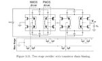
Attached is the circuit of 2-stage rectifier.
I am designing a RFID rectifier. I am referring a IEEE paper for this purpose.
The paper has shown results for both 130nm and 350nm technologies. I have chosen 180nm technology.
So, I expected results in between the above technologies. To my surprise, the results are wierd - undesirable.
Let me explain you the stuff:
I have used the Widths as mentioned in the reference paper. The rectifier rectifies the input ac voltage from 350mV with an efficiency of 50%. So, I expected that I will be achieving atleast 20-30% of efficiency for 500mV to 700mV of input voltage. To my great surprise, I achieved efficiency less than 8%. I tried to use multi stage of rectifier; even then efficiency is less.
The current at the load is around 4uA. I varied the load from 10k to 100K. When load is 100k, current is 4uA. I varied the input voltage from 100mV to 1V (Peak values). The input current is increasing as the voltage is increasing. That is true. But I expected that the current at the input is same, when I go for 2-stage rectifier. I was shocked to see an increase in the ac current at the input end for 2-stage rectifier.
What should I do in order to increase the efficiency? DC load current is always around 4uA. I am able to see the voltage conversion efficiency. But I couldn't achieve power conversion efficiency. What should I do in order to improve PCE for the attached circuit?
Attached is the circuit of 2-stage rectifier.