Continue to Site

Welcome to EDAboard.com

Welcome to our site! EDAboard.com is an international Electronics Discussion Forum focused on EDA software, circuits, schematics, books, theory, papers, asic, pld, 8051, DSP, Network, RF, Analog Design, PCB, Service Manuals... and a whole lot more! To participate you need to register. Registration is free. Click here to register now.

Splitting of Ground plane for Analog signals and DC supply

Status
Not open for further replies.

sreejithpdas

Newbie level 6
Joined
Sep 12, 2012
Messages
12
Helped
0
Reputation
0
Reaction score
0
Trophy points
1,281
Activity points
1,379
Hi,

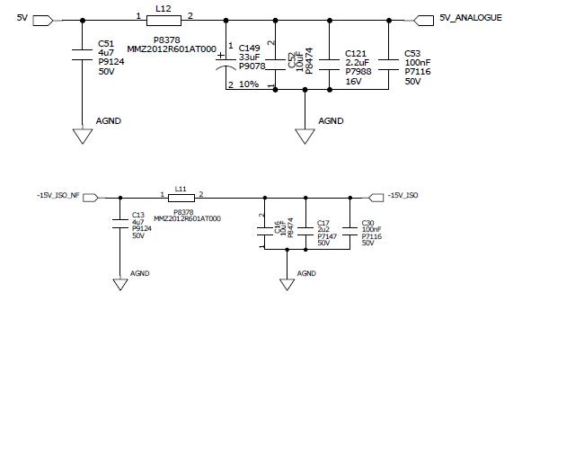
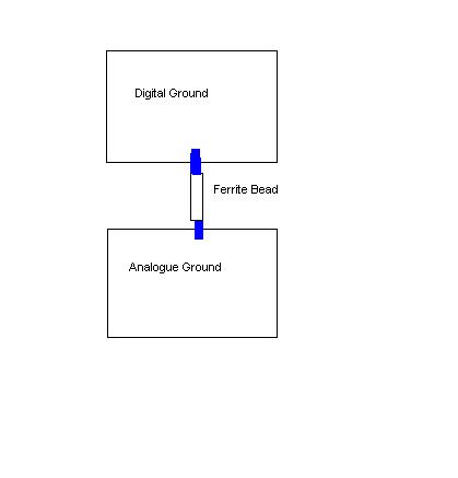
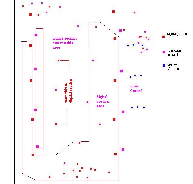
I am a newcomer in RF board design. The analog signal on the board is of 2.4GHz. I am using 1.8V dc supply to the board. Do I need to split my ground plane so as to provide return current path to the analog signal, which then gets separated from the return path of dc current? Is it dangerous to use a single ground plane from an EMI perspective?

Thanks in advance,
Sreejith
 

Hi sree,
for analog and digital separation ferrite bead used right or 0E resistor used ?? keep the bead between analog and digital ground (for separation).better post the snapshot for good understanding.
 

View attachment rf_board.bmpView attachment rf_board.bmp

Kapil,

Attached is the board I am working on. Its a two layer board with routing on both the layers. I have used copper pours as ground on the bottom layer. Analog signal is routed on the top layer, beneath which I have created the analog ground separation. The rest of the board is covered with dc ground on the bottom layer. Also marked the inductor (zero ohm) which is used to connect the ground planes.


-Sreejith
 

Hi sree,
from my point of view,you need to take care for placement and some signal is running in the split plane (please avoid it).give at least 25 mil clearance between analog and digital ground. is there any command ground is there ??

please follow the pcb consideration
 
Last edited:

Thanks Kapil.

I had avoided analog signals running on the split plane. Is the same constraint applicable to the traces which carry dc current also? And I didn't get what you meant by command ground...

-Sreejith
 

sorry chassis ground is there or not ?

- - - Updated - - -

sorry chassis ground is there or not ?
 

I am using OrCad 9.1 for designing this board.
 

Hi,

I have got 4 grounds in my layout. AGND,DGND and SERVO_GND, CHASS_GND. AGND,DGND,SERVO_GND are spread all over the board and I can't able to group the respective grounds together. I am using 8 layers. Could you please tell me if the following PCB stack up is ok for layout and there wont be any EMC issues.

--------------------TOP
--------------------DGND
--------------------SGINAL 1
--------------------POWER
--------------------AGND
--------------------SIGNAL 2
--------------------SERVO_GND
--------------------BOTTOM

Iam using ferrite bead to separate grounds. I can use the ferrite bead only in the top layer. how do i connect the ferrite bead with two different grounds on two different layers. (Layer 2 and layer 5). Using via from ferrite bead to the appropriate layer ?
 

Hi,

I have for 2 power supply. 24V_digital and 24V_servo., 24V_digital is fed through regulator to get +15V and -15V. Could you please also let me know if the below circuit diagram is ok regarding the grounding. 5V,3V3 and 1V8 are from DC-DC Converter which is a DIGITAL_GROUND. But I have used AGND before ferrite bead L12.

Power supply used in my circuit.

+15V_ISO
+15V_ISO_NF
-15V_ISO
1V8
24V_DIGITAL
24V_FUSE
24V_FUSE_NF
24V_SERVO
3V3
3V3_FILTERED
3V3_NF
5V_ANALOGUE
5V_NF
LVDS_3V3


Hi vikash,
From that input,better follow this:
1)conform your placement analog and digital should be seperated as well as Servo section also
2)From that two Power signal which one has High current carrying for example if Servo section has High current carrying capacity better kept it in one plane
3)i think instead of(Layer5)Agnd you should extra add power layer because is not symmetrical.For one layer that means Plane PWR (layer4) not sufficient for distribute power in all layer so you need use Agnd as power you stack-up should be like that

--------------------TOP
--------------------DGND,AGND
--------------------SGINAL 1
--------------------POWER1
--------------------POWER2
--------------------SIGNAL 2
--------------------SERVO_GND
--------------------BOTTOM
 
Hi,

Thank you for your reply. I have decided to use my board stack up as follows

--------------------TOP/Digital power supply
--------------------DGND,AGND
--------------------SGINAL 1
--------------------POWER1/Digital power supply
--------------------POWER2/Servo Power supply
--------------------SIGNAL 2
--------------------SERVO_GND
--------------------BOTTOM/Servo Power supply.

I have got another question. My digital ground and analogue ground are spread all over the board and I wont be able to group them together to do split/mixed plane layout. I have shown a picture of layout which is normally done for all type of boards having AGND and DGND.


Example board picture is my current board layout where the grounds are spread all over the board. Do I need to use via for digital ground and AGND to via through layer 2 (DGND,AGND) for all components ? is it the only possible way ?

 
Hi vikash,
try to change the placement and picture 1 is correct so better follow this. i could not understand second question explain ??
 
Example board picture is my current board layout where the grounds are spread all over the board. Do I need to use via for digital ground and AGND to via through layer 2 (DGND,AGND) for all components ? is it the only possible way ?
Can you eat the cake and still have it?
 

Hi vikash,
try to change the placement and picture 1 is correct so better follow this. i could not understand second question explain ??

My question is how to add copper pour on top layer for the picture I have shown with different grounds. Can I use digital ground flooding for the top layer and add vias for the AGND to connect with layer 2 (AGND) ?

- - - Updated - - -

Can you eat the cake and still have it?

I dont understand your question.
 

That's what we have to call a really bad designed ground plane, I fear. The fissured plane might be appropriate for multiple power rails, if sufficient local bypassing can be provided but hardly for a ground plane.

Most likely a common, continuous ground plane will be better. In many cases, the split ground plane concept involves an error of reasoning, as discussed in previous threads.

If we refer to the topic addressed in the initial post, 2.4 GHz RF, split ground is just a no-no. Every copper pour that's not directly connected or closely coupled to the common ground plane must be expected to work as an unwanted antenna structure, either sending or receiving RF.

Most circuits that have to deal with higher signal frequencies or fast switching (e.g. SMPS) will take advantage from continuous ground planes. The problem is to keep fast and higher level signals from spilling all over the plane. In some cases, e.g. for power supply switchers, a local ground plane above the common plane, connected to it in a single point might be helpful, but without cutting the common plane.
 
Last edited:
Hi,

Thank you for your help.
 

Status
Not open for further replies.

Part and Inventory Search

Welcome to EDABoard.com

Sponsor

Back
Top