hareshsingh
Newbie level 2
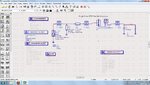
I have simulated half wave rectifier ckt using ADS2009. i have following isssues regarding this.
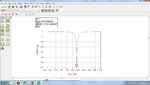
1. i have made the proper matching ckt using smith chart utility for rectifier ckt i.e.my s11 is good enough but still why all power is not going into the ckt.
i know this depends on power level also ,but what is the criterion to do this.
2.whether i should to LSSP to understand this better i.e. SP is not the right thing to do here.
3. i have been looking into agilent application notes , but they never seem to discuss the efficiency of power transfer in such detector ckt.
4. generally what kind of eff.(%) (from input power to load power ) i am supposed to get from such half wave rectifier circuits.
I will really thankful for any kind of help in this regard. i am attaching the schematic , i can provide more detail if needed
regards
haresh