Continue to Site

Welcome to EDAboard.com

Welcome to our site! EDAboard.com is an international Electronics Discussion Forum focused on EDA software, circuits, schematics, books, theory, papers, asic, pld, 8051, DSP, Network, RF, Analog Design, PCB, Service Manuals... and a whole lot more! To participate you need to register. Registration is free. Click here to register now.

SOC encounter Routing power pins of the IO pads

Status
Not open for further replies.

a_mythpi

Junior Member level 1
Joined
Mar 17, 2013
Messages
16
Helped
1
Reputation
2
Reaction score
1
Trophy points
1,283
Activity points
1,410
Hello,

Can anyone please advice me on the routing of power pins in the IO pads. I used the global net connect command to connect the power pins to net vdd and net gnd. Then I tried sroute with pad pins. But I am getting hole violations . I am not really sure the order in which the routing must be done. Please provide me with a sample code for executing the power routing command.

Thanks

Amith
 

The power routing should be done during the floorplan step, with adding, addstripe or edit route (shift + a) and this a manual step.
Only the standard cell, could be route with sroute, properly, for macros and pad, it is better to use the command indicate before.
Other command could be used to route the second power net for multi -power std cell, like level shifter or flip-flop with retention.
 

Hello.

thank you for your reply. I have around 100 pads out of which 16 are power / ground pads. How do I route this to the power rings outside my core design manually. Also I see in the design browser that there are a number of p/G nets for every IO pad. How do I route these pins appropriately?

- - - Updated - - -

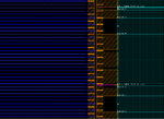
Here are the two snapshots of the eroor I am getting when i route using sroute..
IOfiller_1.pngIOfiller_2.png
 

the PG pin for each IO pads will be connected by the filler pad?
for the 16 PG pads, you could easily connected them manually (shift+a, "e" to open the gui to control the add write tool).
 
Hi.

How do you connect the pins Manually? I mean which metal is to be used and also I donot know how to use SOC encounter tools to manually create metal layers. to connect them
 

shift+a, "e" to open the gui to control the add write tool, as indicate in my previous reply
 

Status
Not open for further replies.

Part and Inventory Search

Welcome to EDABoard.com

Sponsor

Back
Top