Continue to Site

Welcome to EDAboard.com

Welcome to our site! EDAboard.com is an international Electronics Discussion Forum focused on EDA software, circuits, schematics, books, theory, papers, asic, pld, 8051, DSP, Network, RF, Analog Design, PCB, Service Manuals... and a whole lot more! To participate you need to register. Registration is free. Click here to register now.

DeEmbedding 0805 SMT results

Status
Not open for further replies.

darcyrandall2004

Full Member level 1
Joined
Feb 1, 2009
Messages
97
Helped
3
Reputation
6
Reaction score
0
Trophy points
1,286
Location
Perth, WA, Australia
Activity points
2,099
Hello,

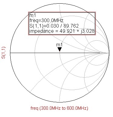
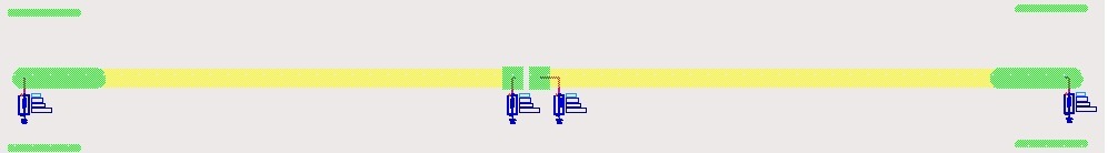
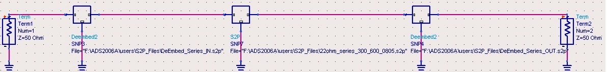
In an effort to improve the accuracy of my RF design, I have created a PCB for measuring 0805 smt components in a series and shunt configuration. See below.


Using momentum I created a layout component of the PCB. I measured the S parameters of a 22ohm resistor placed between port 1 and 2 using the VNA. I then deEmbed the component from the PCB using ADS.


I would expect to read an input impedance of 72 ohms when a 22ohm series resistor is placed between port 1 and 2 of the VNA. Instead I measured roughly 72 ohms but strangely a series 10pF capacitance.

6190244000_1367212144.jpg


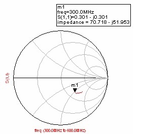
Does this value of 10pF parasitic series capacitance sound correct? If this 10 pF parasitic capacitance is always present then it will severly limit the choice of series components I use.


Like wise a shunt 47ohm resitor measured with 1 port of the VNA shows a 35pF series capacitance parasitic. I would have expected a parasitic series inductance due to the via between the resistor and the ground plane.

5044545200_1367212199.jpg


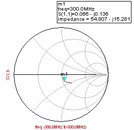
Do these results sound correct?

Note: My pcb is 0.8mm FR4 with 1.4mm wide tracks, 35um thick copper and a complete ground plane on one side. (ie characteristic impedance of 50ohm)

Thank you
 

Something funny is going on. How did you acquire the deembed components? Measured or simulated?
 

1.I imported the PCB DXF file into ADS Layout (Momentum).
2.I specified all the parameters such as thickness of the substrate, permittivity etc.
3.I added a bunch of ports to the layout at points where the SMA connectors sit and the 0805 components are mounted.
4. I measured the S parameters from port1 SMA connector to port2 0805 component. I then measured the S parameters from the other pad of the 0805 component to the port4 SMA connector.
5. I wrote these S parameters to two .s2p files. I use these .s2p files for the DeEmbed components.

What results would you expect to see in terms of parasitic capacitance and inductance for a shunt and series measurement?
 

No this is not correct results, if system is calibrated, and the resistor not is piggybacked by a capacitor. Maybe very wrong parameters entered in ADS but that is easy to check. Most likely is it a problem with VNA calibration.

If the VNA is correct setup is it fully capable to do this kind of measurements without need for ADS.

Calibrate the unpopulated PCB for open, load and short and then measure S11 for any component shunted to ground.
Do a two port calibration and it is also possible to measure serial impedance with PCB losses excluded.
 
  • Like
Reactions: FvM

    FvM

    Points: 2
    Helpful Answer Positive Rating
I have been reading agilent application note Application Note 1364-1. According to this document I need to model the SMA connectors and the parasitic interface to the PCB.

I have attempted to determine the parasitic components but unfortunately ADS does seem to be able to produce a solution.

1.jpg

- - - Updated - - -

I have been reading agilent application note Application Note 1364-1. According to this document I need to model the SMA connectors and the parasitic interface to the PCB.

I have attempted to determine the parasitic components but unfortunately ADS does seem to be able to produce a solution.

1.jpg
 

the resistor has solder pads. Those pads have a capacitance to ground. So, yes, there will be some capacitance shown on the smith chart. But a very careful de-embedding is needed. Did you use microstrip cal standards?
 

It looks like you are struggling hard to make a basically simple thing (calibrating a test fixture) complicated.

You can of course calibrate the VNA to the cable ends, make an accurate s-parameter description of the test fixture and calculate the DUT s-parameters by "de-embedding" methods. But no RF engineer will do this. Even a fairly accurate in-circuit calibration of the test fixture will achieve better results.

Choosing a reasonable reference plane is essential however. If you are measuring a 0805 resistor in a 1.4 mm stripline, why should you place the reference plane cut before the pads and get an extra pad capacitance in the measurement? If the pads are included in the text fixture's transmission line, the capacitance effectively cancels out.
 
Did a very simple measurement.
1. Calibrated VNA.
2. Connected VNA to a dual side PCB equipped with SMA connector and 30 mm long 50 Ohm transmission line.
3. Adjusted electrical delay at VNA for the open ended transmission line.
4. At the end of transmission line was a 0603 47 Ohm resistor soldered to ground (no real pads).
Measured S11 Smith chart:
test2.jpg
Not perfect but ok. However if I had measured a capacitive loss of 10-20 pF, had a alarm-bell ringed, as that corresponds to a pad in size maybe 10-20 mm in diameter.
 
  • Like
Reactions: FvM

    FvM

    Points: 2
    Helpful Answer Positive Rating
Exactly, you're totally right! At 300MHz the SMA to microstrip interface shouldn't be a problem. I expect you have the SMA soldered directly on the PCB, without any wires? Even the 0805 pads shouldn't make any difference at this low frequency. 10pF is huge. Why don't you post a photo of your circuit?
 

Below is my Advantest VNA with S parameter test set. I have 0.5m Jyebao cables (not sure of the spelling). The cables have a DC block on the ends. Measurements were taken at -35dbm
1.jpg

Shown here is the cheap SMA RF calibration kit I got from RFSHOP.com.au supposedly good upto 5GHz.
4.jpg

Here is the PCB I use to measure the 0805 components. It has SMA connectors. Ground is on one side only. The SMA connectors are soldered to ground on the bottom of the board. I have included the ability to perform a calibration using the PCB (SOLT). I tried this however and achieved poor results hence the reason for trying DeEmbedding. The problem with making your own standards is that you also require the standard definition tables to meaure against so you can determine your error.
2.jpg
3.jpg

I calibrated my VNA at the connector then measured the 22ohm series 0805 resistor on the PCB between port 1 and port 2 (No DeEmbedding). Below are the results. This time I measured 32pF parasitic capacitance at 300MHz.
6.jpg

I then performed measurement on the 47ohm Shunt resistor using just port 1 and I measured a reasonable 1.5nH inductance.
5.jpg

- - - Updated - - -

To be thorough I measured the 22ohm resistor in shunt on the PCB with no DeEmbedding. Note: electrical delay = 0ff
This time at 300MHz its off by 5 ohms and 10nH.
7.jpg
 

I have attached the substrate definition I have used aswell.
8.jpg

- - - Updated - - -

Even a fairly accurate in-circuit calibration of the test fixture will achieve better results.

I have previously tried performing an in circuit calibration of the text fixture, it was innaccurate. What do I use for the standard definition tables? The VNA I have only has standard definition tables for SMA and N type calibration standards. I would need a standard definition table for my PCB.

I am hoping DeEmbedding will provide more accurate results.
 

Guess it is a problem with electrical delay. Check electrical delay is correct set:
Measure S11 open, PCB connected but no components. Repeat for S11 short, with aid of a short wire connected to ground.
If electrical delay is correct set should Smith chart show a single dot and almost no reactive load. If not, manually adjust delay and check again.

If it not is possible to get reasonable well defined dots, check that cables and connectors not are faulty. For example can SMA connectors by worn out, center pin bent..
Also check that calibration kit seems correct by visually inspection, compare with connecting a SMA open if calibration kit parameters are correct set in VNA.

If electrical delay seems correct adjusted, then verify that only minor reactive load can be seen for different resistor values when measuring S11 and S21 (and later more interesting, verify calibration by measuring reactive components)

If possible I use predefined calibrations standards, but also have my own calibration standards to be able to do in circuit calibration.
For example requires some measurement that a very thin, flexible and lossy coaxial cable is used when measuring inside cellphones as there not is space enough to route a thicker cable.
Other reasons to do in circuit calibration is when parts of in phone existing PCB traces must be included in calibration. Maybe not a big problem at 600 MHz and short traces but at 2.4GHz can correct calibration be the difference between if a inductor or capacitor should be added to a network.

Have no experience from Advantest and guess it can differ a lot between different brands of VNA, but setting up my own VNA calibration parameters is not so complicated if not too high precision is required.
My precision requirement is in the range that I want an error less then one E12 step, to be able to select correct component values for filters and impedance matching network.
What do I use for the standard definition tables?
Can only tell my procedure, which can be different for another typ of VNA:
First must you know what it is you want to define, which probably is depending on what types of job you want to do.
In may case I often solder a semi rigid 100 mm long cable in an existing PCB with intention to make an embedded antenna, starting from the point where the cable is soldered.. Other end of this cable have a SMA connecto, connect to a low loss cable and VNA. My first need of definition point was therefore the end of this coaxial cable and upper frequency limit 3 GHz.
I have done five exactly similar cables loaded to shield with:
1. short
2. open
3. 4*200 Ohm parallel 0402
4. 4.7 nH Murata 0402 15HS
5. 4.7 pF Murata 0402

Set VNA to span 2-3 GHz
Select defining a new cal.standard and sett all offsets and reactive values to "0".
Make a SOL calibration with this setup and the cables 1-3.
Set electrical delay with cable 1 and 2. No error offset should seen between cable 1 and 2.
Measure cable 4 and adjust Open->C0 for best correct reading compared with from by manufacturer given S11. (I have done a simple software that does this step automatically.)
Adjust C1 for best "tilt"
Verify 50 Ohm load and if needed adjust Load->C0.
Repeat and if needed fine adjust remaining parameters.

A similar coaxial cable is then soldered in a PCB, and electrical delay adjusted by a knife at PCB and it now gives a relative correct reading.

This is a very homebrewed setup with several limitations. Use at your own risk.
 
Last edited:

I will investigate what sort of accuracy I can get with electrical delay and post the results.

E Kafeman would you mind measuring a 22ohm resistor between port 1 and port 2 of your VNA and posting the results?
Without DeEmbedding I received similar results to you with a 47ohm shunt to ground. I am curious to see if you get similar results when you measure a 22ohm resistor between port 1 and port 2 on your PCB.

Thanks
 

Why do you have the relative permeability of FR-4 set to 4.5? It should be 1. Also, set the loss tangent of the relative permittivity to 0.025.


As far as I can tell (doing a linear simulation of your circuit from the photo), all these measurements are correct:

* I calibrated my VNA at the connector then measured the 22ohm series 0805 resistor on the PCB between port 1 and port 2 (No DeEmbedding). Below are the results. This time I measured 32pF parasitic capacitance at 300MHz.
*I then performed measurement on the 47ohm Shunt resistor using just port 1 and I measured a reasonable 1.5nH inductance.
* - - Updated - - - To be thorough I measured the 22ohm resistor in shunt on the PCB with no DeEmbedding. Note: electrical delay = 0ff
This time at 300MHz its off by 5 ohms and 10nH.

I guess your delay offsets were wrong when deembedding.
 
Last edited:
Measured impedance with a 22 Ohm resistor in serial.
It is a in place calibration, a bit better performed then last one that was a SMA-kit calibration. This in place calibration is a kind of deembedding as test PCB was included in calibration procedure. Electrical delay was also manually set. The PCB is else just something from my junkbox. Do not even remember if transmission line was calculated at all.

For the measured result, reactive part is mainly inductive, guess it is due to delay in the resistor and 600 MHz is a bit too low frequency, so stray capacitance is not yet any problem.
S21_22_Ohm.jpg
No visible markers this time, as they else totally hided the measurement curve.
 
After correcting the permeability and tangent loss I was able to successfully measure the 47ohm shunt resistor and 22ohm series correctly. Thanks everyone for their help. ADS also managed to optimise the values for L and C for the SMA connectors over a small frequency range.

Thank you

6318961400_1368189507.jpg
 

Status
Not open for further replies.

Part and Inventory Search

Welcome to EDABoard.com

Sponsor

Back
Top