Continue to Site

Welcome to EDAboard.com

Welcome to our site! EDAboard.com is an international Electronics Discussion Forum focused on EDA software, circuits, schematics, books, theory, papers, asic, pld, 8051, DSP, Network, RF, Analog Design, PCB, Service Manuals... and a whole lot more! To participate you need to register. Registration is free. Click here to register now.

Various Electronic Analysis Questions

Status
Not open for further replies.

danny davis

Banned
Joined
Mar 1, 2013
Messages
627
Helped
0
Reputation
0
Reaction score
0
Trophy points
1,296
Location
Hollywood
Activity points
0
The solid state relay is powered by 120 volts AC , the signal of the solid state relay goes direct a controller PIN

What does the solid state relay do?

Solid State Relay pic#1.jpg

Op-Amp Detector, What does it do ? for logic circuits? it takes an input signal and does what?

Op-amp Dector circuit pic#1.jpg

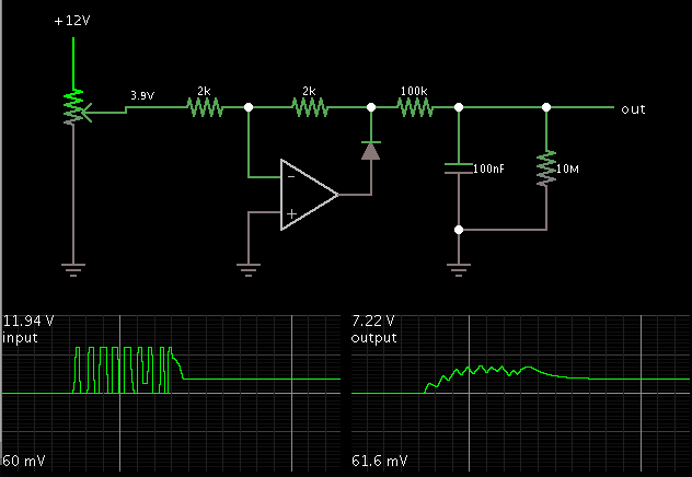
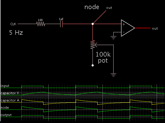
Here is an RC network in the feedback section of an op-amp , what does it do?

RC feedback network pic#1.jpg

This IC voltage Detector, goes direct to the Micro-controllers RESET pin, what does the IC voltage detector do? once the VCC is to low it Resets the Micro-controller?

If there is a short and the VCC is low all the time , it's just going to keep Resetting the Microcontroller right?

Voltage Dector for Microcontroller.jpg

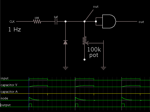
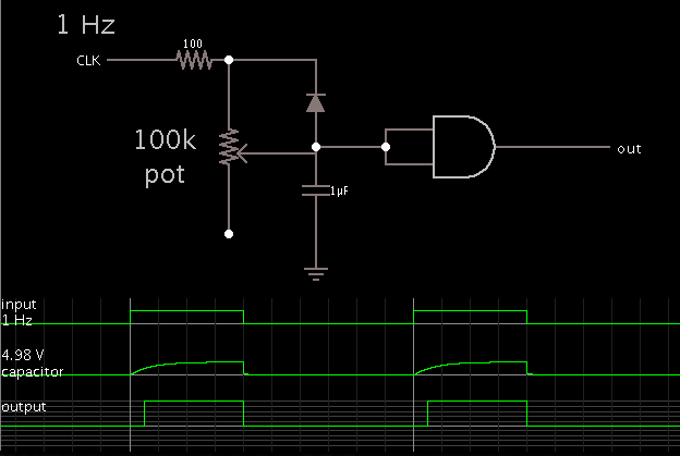
What does these LF13333N Switches do?

When they have an square waveform on the input pin of a LF13333N the output of the LF13333N switch changes the Amplitude of the square waveform i have noticed

LF13333N Switch pic#1.jpgLF13333N Switch pic#2.jpg

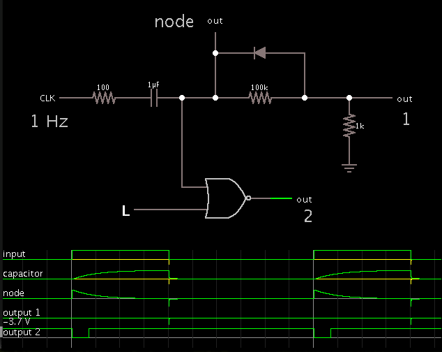
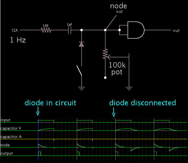
What does the Diodes do? The Nor gates have these Diodes for what?

Nor gate with Diodes pic#1.jpgNor Gate with Diodes Pic#2.jpg
 

Image 7 looks like it might be a one-input bistable multivibrator. Two symmetrical NOR gate arrangements, which are made to change to the opposite state whenever a pulse comes from the upper left. Pulse-on, pulse-off.

Hence image 8 shows two bistable multivibrators. I could be wrong.

Diodes might ensure current goes one way and not the other. Or to isolate output of one device from the output of another device.

If there is a short and the VCC is low all the time , it's just going to keep Resetting the Microcontroller right?

Re image 4. When the microcontroller's reset pin is pulled low, it causes the device to go into limbo for as long as the pin is low. The device does not restart until the pin goes high. (From seeing the way my Commodore computers act when I pushed the reset button.)
 

What does those peak detector op amps do for digital TTL or CMOS logic signals? what are the peak detector op amps used for?
 

1.) The Diodes are for when the NOR gate is in the OFF state
When the NOR gate is in the ON state is a time constants from the capacitor and resistor and when the OFF state is doesn't go through the resistor, is goes through the diode

2.) The Diodes protect it from creating a short circuit since the NOR gates are connected in Parallel

Nor gate with Diodes pic#1.jpgNor Gate with Diodes Pic#2.jpg


This is a comparator op-amp
When a Logic HIGH is on the input , the output is a LOW
When a logic LOW is on the input, the output is a HIGH
The Diode is to set the hysteresis

Voltage Dector for Microcontroller.jpg

I'm not sure when they didn't use a Schmitt invertor instead

I guess the diode sets up a DC offset voltage?
 

Since U19 sends either a high or low, there should be no need for a Schmitt trigger.

It looks as though the diodes are to prevent the capacitors from discharging, once charged. One capacitor holds a charge until there is a change of state. Then it discharges, and the other capacitor charges.

Each pulse from U19 causes a change of state. Maybe it receives the Power-on, power-off pulse from a remote control? Or the caps lock button?

It would be easier to grasp operation, with the help of a simulator which supports 3-input logic gates. (Falstad's does not.)

--------------------

One thing to consider when a component does not have an obvious purpose: It may have been installed as a workaround, to prevent some problem that happens occasionally and/or unpredictably. I suspect commercial circuit boards have many of these. We can puzzle ourselves over many components. Bypass caps, safety resistors, ESD zener diodes, steering diodes, crowbar transistors, etc.
 

I mean they used an op amp as a comparator with a Diode , to do what?

What does this circuit do?

- - - Updated - - -

I posted the wrong pictures he is the right one

This is a comparator op-amp
When a Logic HIGH is on the input , the output is a LOW
When a logic LOW is on the input, the output is a HIGH
The Diode is to set the hysteresis

Op-amp Dector circuit pic#1.jpg
 

I mean they used an op amp as a comparator with a Diode , to do what?

What does this circuit do?

- - - Updated - - -

I posted the wrong pictures he is the right one

This is a comparator op-amp
When a Logic HIGH is on the input , the output is a LOW
When a logic LOW is on the input, the output is a HIGH
The Diode is to set the hysteresis

View attachment 90287

The schematic could act as a peak detector if the capacitor is only allowed to discharge very slowly.

I see it working as an averager in simulation:


The capacitor quickly discharges back through the input resistance, more than through the 10M resistor.

This does not mean I know what its purpose is in the whole picture.

----------

The link below will open falstad.com/circuit, load my simulation, and run it on your computer.

You'll see a slider at the right. Move it and you move the potentiometer.

https://tinyurl.com/d6sqygl
 

yes my electronic book say they same thing that it's maybe a peak detector to HOLD the peak voltage on the cap

In general do you know what peak detectors are used for in logic circuits? why do they use peak detectors for what purpose?

- - - Updated - - -

I see it working as an averager in simulation:

What you mean by averager? how so?
 

What you mean by averager? how so?

At first I moved the potentiometer up and down quickly. The capacitor could not respond fast enough, but could only trace a triangle wave at an average level between the extremes.

Then I let the potentiometer settle. The capacitor settled at the same value.

I would not call my schematic a peak detector. A peak detecting capacitor drops very slowly from the peak value (until it is deliberately discharged).

My schematic probably acts differently from yours, since mine does not include the unseen components.

yes my electronic book say they same thing that it's maybe a peak detector to HOLD the peak voltage on the cap

In general do you know what peak detectors are used for in logic circuits? why do they use peak detectors for what purpose?

Example, to get input from a large number of analog devices, and hold each reading for a while while a decision-making unit queries them one at a time. If one sensor gives a high enough temperature reading, then it might register as logical 'high', and cause the air conditioning to turn on.
 

oh ok thanks

What do the 2 resistors do? the ones I circled, I see these a lot in logic circuits, It's not just a voltage divider, its like it's pull up the logic signal to a reference zero

Does the 2 resistors level shift the logic signal?

Does the 2 resistor Clamp the Logic signal to clip at a certain voltage?

Why is the VCC +5 and the VDD - 15 volts? why not -5 volts or zero volts, why -15 volts?

Logic Resistors pic#1.jpg

- - - Updated - - -

The High state is +5 volts and the low state is -15 volts, why not zero volts? why is it -15 volts?
 

oh ok thanks

What do the 2 resistors do? the ones I circled, I see these a lot in logic circuits, It's not just a voltage divider, its like it's pull up the logic signal to a reference zero

R97 goes between the output of one IC and the input of U19. Either it is a safeguard just in case a short occurs somewhere, or it shares partial influence with a component in the wire going off to the right.

R103 & 102 & 96, set a level of 1.94V at the op amp input. I don't know why R96 (1K) needs to be added in series with R102 (100k). (If R102 were alone the level would be 1.97V.)


Does the 2 resistors level shift the logic signal?

Does the 2 resistor Clamp the Logic signal to clip at a certain voltage?

Yes, they set a default level at the op amp input when no signal is coming through R95:2 (1k).

Why is the VCC +5 and the VDD - 15 volts? why not -5 volts or zero volts, why -15 volts?

Most likely the op amps need a negative supply as well as a positive, and a -15V polarity is already available on the board, so the designer used that for convenience.

It need not be a symmetrical supply... meaning it need not be -5V.
 

Thanks for the info

There is only an RC time delay only on the HIGH logic state , the low logic state goes through a bypass diode straight direct to ground

Why are these RC time delays used for logic HIGH states?

Logic High RC network#1.jpgLogic HIGH RC time pic#2.jpgLogic HIGH RC time pic#3.jpg
 

I don't trust my mind to analyze these correctly so I used a simulator. Nothing prevents you from doing the same. Falstad's becomes surprisingly easy to use after a while.

However I do not mind. These schematics are interesting because they are a clever and inexpensive way to do jobs which we might ordinarily think are for a 555 timer IC. They work on a similar principle as the 555.

Schematic #1:


This is a one-shot. When the input goes high, the capacitor creates a short spike.

The diode absorbs the negative spike caused when the input goes low. The logic gate is exposed to a slight negative pulse.

----------------

Schematic #2:


When the input goes high, the output delays momentarily, then goes high.

When the input goes low, the output immediately goes low.

-------------------------------

Schematic #3:


When the input goes high, the output #2 delays momentarily, then goes high. It stays high throughout, and goes low when the input again goes high.

Output #1 creates a negative-going spike when the input goes low.

The logic gate is exposed to a negative polarity, something not recommended in operating guidelines.
 

Here is the RC networks , only is for the HIGH logic state and the LOW logic state goes to the diode

RC network for HIGH logic state pic#1.jpgRC network for HIGH logic state pic#2.jpgRC network for HIGH logic state pic#3.jpg

- - - Updated - - -

What I don't understand is why does the HIGH and only the HIGH logic state need a RC time delay?

One of the diodes goes to ground and the other diode in pic#3 doesn't, it bypasses the RC network, how are they different?
 

What I don't understand is why does the HIGH and only the HIGH logic state need a RC time delay?

Our intuitive sense makes us think of a positive pulse as the 'active agent'. Whereas a 0V state 'does nothing'. It is similar to the binary opposites yes/no, on/off, 1/0. It seems logical to our minds (even though some electronic devices use reverse logic).

One of the diodes goes to ground and the other diode in pic#3 doesn't, it bypasses the RC network, how are they different?

These diode-capacitor-resistor combinations can be made to do all sorts of waveform modification.
Upward-going and downward-going. The purpose might be to time-align one signal with another elsewhere, or eliminate jittery pulses, or to create a time-window of a certain length. Etc.

As for the diode to ground... in this case it is not for pulse extending or delaying. It is needed as a safeguard. It absorbs negative spikes of -4 or -5 V. Without it the IC could be damaged.

Simulation comparing waveforms with and without the diode:


It started with the switch closed. The switch was opened after the second pulse.

Look at the 'node' trace and you will see negative spikes being produced when the diode is out of the circuit.
 

Thanks for your info and help

I do see those negative spikes, what is causing them or producing those negative spikes?
 

Thanks for your info and help

I do see those negative spikes, what is causing them or producing those negative spikes?

A voltage is applied to the capacitor, charging it in one direction.

The input suddenly reverses state, sending current in the opposite direction through the cap.

The capacitor adds its charge as well. The result is a spike that could be negative, or it could be as much as twice the incoming voltage, depending.

My video on Youtube portrays this action visually, as an animation.
It shows the capacitor charging and discharging, with different waveforms.

www.youtube.com/watch?v=eIWEU4pObJw
 

But its not an AC signal, it's a logic low to high , the low should be zero volts , so where is the negative spike coming from logic signals?

- - - Updated - - -

But its not an AC signal, it's a logic low to high , the low should be zero volts , so where is the negative spike coming from logic signals?
 

But its not an AC signal, it's a logic low to high , the low should be zero volts , so where is the negative spike coming from logic signals?

This is one of those tricks we make use of frequently in electronics, almost without thinking about it.

A series capacitor can turn a DC waveform into AC, blocking the DC component. It is commonly done in audio amplifiers.


The many scope traces make it possible to see what's going on.

It's even easier when you watch the animated simulation. Click link below.

https://tinyurl.com/bsnohdb

It shows current bundles going back and forth through the cap.
 

I understand the Capacitor voltage ramping up and down , but the NODE puts the capacitors discharge voltage into a negative cycle below the zero point

When the Capacitors voltage is charging and discharge it says above the zero reference

When the NODE is charging it is in the positive cycle and when the NODE is discharge it's in the negative cycle below the zero point

What makes it go below the zero point into a negative cycle? is it because the resistance sets up a DC offset at the NODE point?
 

Status
Not open for further replies.

Similar threads

Part and Inventory Search

Welcome to EDABoard.com

Sponsor

Back
Top