Continue to Site

Welcome to EDAboard.com

Welcome to our site! EDAboard.com is an international Electronics Discussion Forum focused on EDA software, circuits, schematics, books, theory, papers, asic, pld, 8051, DSP, Network, RF, Analog Design, PCB, Service Manuals... and a whole lot more! To participate you need to register. Registration is free. Click here to register now.

Is the deep nwell process allowed in TSMC65 technology?

Status
Not open for further replies.

Alex Liao

Member level 4
Joined
Apr 8, 2013
Messages
75
Helped
2
Reputation
4
Reaction score
2
Trophy points
1,288
Activity points
1,991
I placed a nch (nmos) in a pw and pw is on a deep newll which is within the nwell on a p-substrate. Please refer the attachment for reference of the placement.

I cannot pass the LVS and have information like this:
Error Message:
Nothing in Layout; corresponding cells could not be identified;Nothing in Layout.
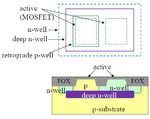
D-nwell.png
 

Depending on your PDK, isolated nmosfets probably need additional recognition layers to be recognized as such by the extraction tool.
Read your PDK docu!

If TSMC supports the deep nwell option in 65nm tech you should ask MOSIS or TSMC themselves.
 
Status
Not open for further replies.

Part and Inventory Search

Welcome to EDABoard.com

Sponsor

Back
Top