Continue to Site

Welcome to EDAboard.com

Welcome to our site! EDAboard.com is an international Electronics Discussion Forum focused on EDA software, circuits, schematics, books, theory, papers, asic, pld, 8051, DSP, Network, RF, Analog Design, PCB, Service Manuals... and a whole lot more! To participate you need to register. Registration is free. Click here to register now.

Laying out a high current, high frequency inverter chain in 0.5u CMOS

Status
Not open for further replies.

mtwieg

Advanced Member level 6
Joined
Jan 20, 2011
Messages
3,835
Helped
1,310
Reputation
2,626
Reaction score
1,405
Trophy points
1,393
Activity points
29,370
This past semester I've been taking a CMOS course in which we're using Cadence for designing low power mixed signal ASICs. This is nice and all, but I was thinking I could actually use a custom ASIC in my actual research (which deals with switchmode RF amplifiers). Basically one frustrating problem I face is how to effectively hard-switch FETs at high frequencies (like 120MHz). Ideally I want a nice clean 0-5V square wave for gate drive, but there aren't any off the shelf components meant to do this. The best approach I have is to use a bunch of high speed CMOS logic gates in parallel, but this doesn't seem to effective either. So I'm thinking I should try my own ASIC solution. Basically I want to make a ridiculously high power and high speed logic inverter. Fortunately my school gets to do a few free fab runs a year, so it wouldn't cost an arm and a leg to try...

My rough specs are as follows:
0.5um ONsemi process
Switching frequency: 125MHz
5V supply, r-r output swing
Drive 250pF load with tr/tf of <2ns (so at least 600mA of peak output current)
Overall delay is not a big deal, so long as the delay does not vary too much. But I don't want the duty cycle to be distorted significantly (+/-10%)

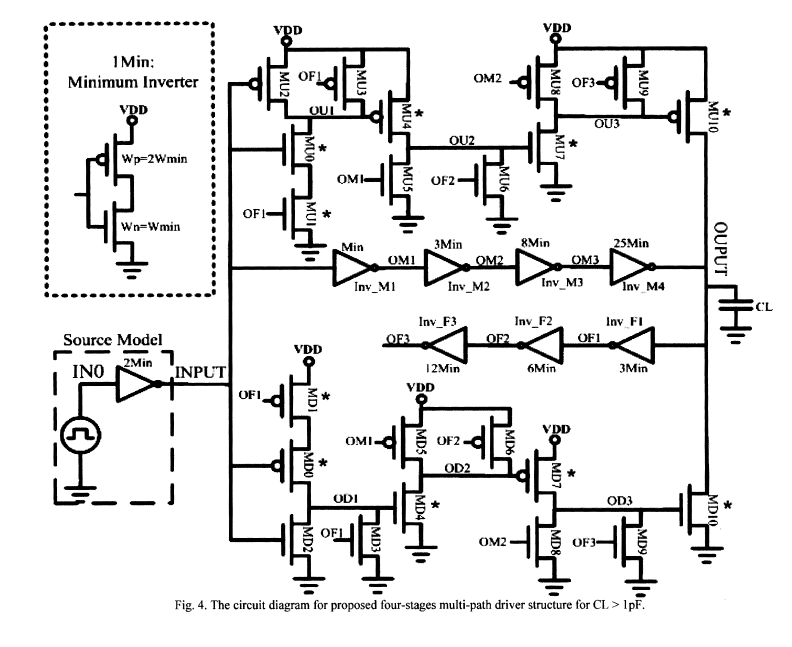
So what sort of issues would I run into? I have a feeling that I'll have to fan my inverter chain into many parallel chains which combine at the output (maybe each with their own pad, for lower bondwire ESL). Also with such large devices will I have to worry about shoot through current? Will I need some sort of modified inverter circuit to prevent this? Does this sound like total nonsense?
 

Really? Nothing at all?

After looking around I did find one interesting relevant paper. They drive 4pF with rise/fall times of ~100ps, so 40mA out peak. Here's a shot of the circuit they use:


So if I wanted to adapt a similar approach to my problem, I have a few questions:
Their design uses Vdd of 1V, and I want Vdd=5V. They also use 65nm while I would use 0.5um. I think that means that in my design, I will have much more margin for gate drive of my transistors. I'm wondering if this also means cross conduction will be a greater problem at 5V...
I need about 10x more drive power than their specific design offers, so should I just make the cascade longer, or put multiple copies in parallel? What are the tradeoffs involved with such approaches?
They only simulate their design at the circuit level, so they don't mention anything about layout. What kind of routing techniques should I use to keep supply rail and output inductances low? If I end up making such a thing, I can hopefully get a flip chip package...
 

This is somewhere between a Class E PA and a DC-DC
converter output stage, I guess.

You definitely will want some sort of anti-shoot-through
to keep from burning all your power before it gets off chip.
I use "ballistic" (designed asymmetry) mostly, and just
hand-fiddle the taper until it lines up right at slow/hot.
I'd say you want both the final and both the N and P
predriver to be near zero shoot-through.

I would use multiple bond wires and try to fly power &
ground into the interior of the power stage if allowed.
Using separate bonds for the high and low side drive
legs could be a good idea too, helping isolate the
output dV/dt from the device that's supposed to be
turning off (some).

125MHz, full swing is going to be a challenge. On 0.5um
SOI I've gotten to 1GHz full swing in very limited logic,
400MHz chip scale clocks, but nothing like a power
driver and had to stick to a 2:1 taper to make it go
(of course if you're not stuck with MIL temp range,
that's a nice bonus). I think on JI technology you are
at about the same place. On that same 0.5 SOI node
others have made 2GHz Class E PAs at about 30%
efficiency. Using this node I've done DC-DCs to 10A
and 85% efficient at 5MHz, but it's starting to fade
there. This is not a 5V rated technology, but 3.3V.

Also forget 5V in a 0.5um gate length unless they
managed to engineer the hell out of the drains. Or
expect to be using a thick oxide I/O device with a
longer than the 0.5um advertised L.

Your alternative is to go to a shorter node like
0.25um, and stack FETs. This is as low as you can
go and stand off 5.5V with a stack of 2. Probably
pushing the well voltage limits (at least, rated).
You will gain a lot of speed but also need to split
the powertrain into high side and low side, make a
stiff-enough midrail, have level shifting that comes up
clean and so on.
 
  • Like
Reactions: mtwieg

    mtwieg

    Points: 2
    Helpful Answer Positive Rating
Thanks for the reply, I'm going to take this bit by bit...
This is somewhere between a Class E PA and a DC-DC
converter output stage, I guess.
Ultimately I'm trying to drive a soft switched class D RF amplifier (not to be confused with class S PWM amplifiers...). The gate driver should be entirely hard switched though.
You definitely will want some sort of anti-shoot-through
to keep from burning all your power before it gets off chip.
I use "ballistic" (designed asymmetry)
Never heard these terms before, could you elaborate a bit?
I'd say you want both the final and both the N and P
predriver to be near zero shoot-through.
Might it also be necessary for some preceding stages to guard against shoot through? How can I judge whether it's necessary or not for a given stage?
I would use multiple bond wires and try to fly power &
ground into the interior of the power stage if allowed.
Using separate bonds for the high and low side drive
legs could be a good idea too, helping isolate the
output dV/dt from the device that's supposed to be
turning off (some).
I have a feeling I won't be able to get MOSIS to do this for me (we get a pretty cheap university deal with them, and I think they only do pad/pin bondwiring, no internal jumper bonds).
Also forget 5V in a 0.5um gate length unless they
managed to engineer the hell out of the drains. Or
expect to be using a thick oxide I/O device with a
longer than the 0.5um advertised L.
This process is typically used by my university for 5V designs, and I believe they use minimum sized devices for logic elements. So I'm pretty sure it's good for 5V operation. I think MOSIS rounds up the channel lengths to 0.6um though....
 

Status
Not open for further replies.

Part and Inventory Search

Welcome to EDABoard.com

Sponsor

Back
Top