Continue to Site

Welcome to EDAboard.com

Welcome to our site! EDAboard.com is an international Electronics Discussion Forum focused on EDA software, circuits, schematics, books, theory, papers, asic, pld, 8051, DSP, Network, RF, Analog Design, PCB, Service Manuals... and a whole lot more! To participate you need to register. Registration is free. Click here to register now.

Feko_reflected and REFRACTED waves problem. Trihedral corner reflector simulation.

Status
Not open for further replies.

Iskrinka

Newbie level 4
Joined
Nov 12, 2012
Messages
7
Helped
0
Reputation
0
Reaction score
0
Trophy points
1,281
Location
Ukraine
Activity points
1,336
Hello!
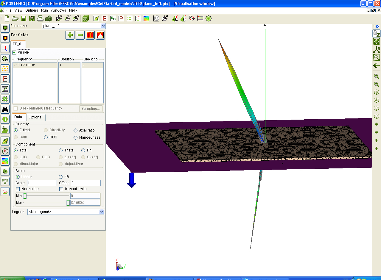
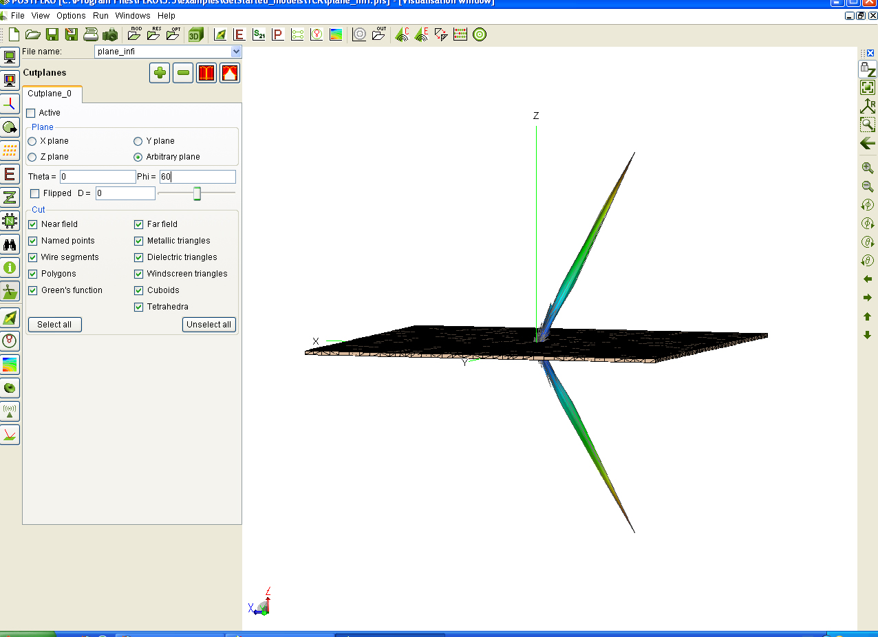
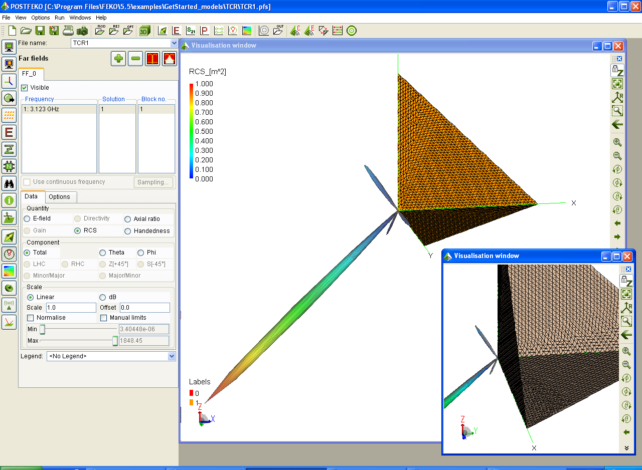
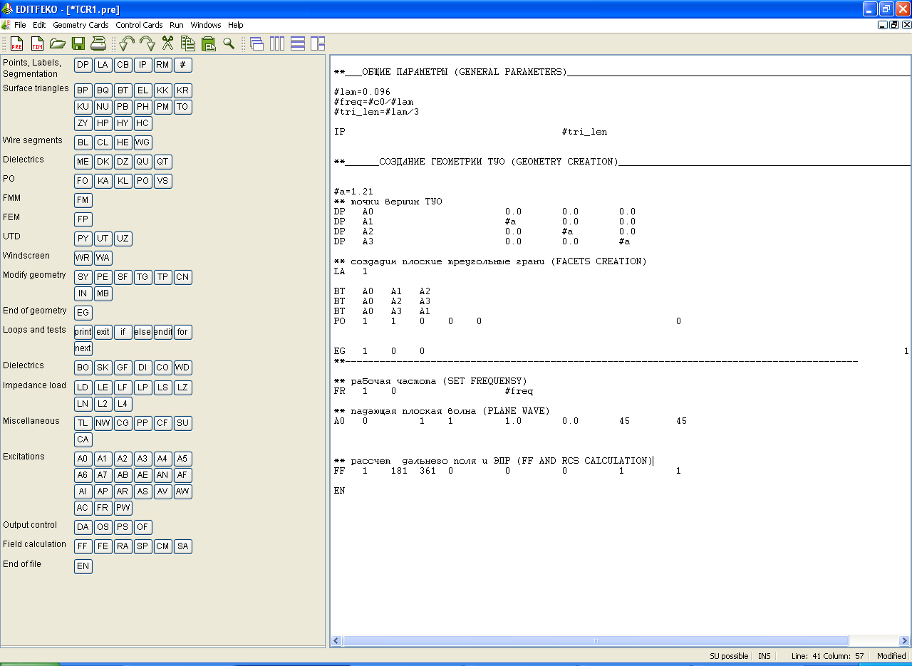
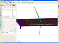
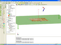
My task is to simulate trihedral corner reflector using Feko, to build backscattered field and to calculate RCS of that one. But I am not experienced user, so I have started with simulation of one metal plane. As a source I have chosen a plane wave. I have made this model in both CADFeko and EDITFeko, BUT(!) when I ran POSTFeko, I have seen, that falling wave passes through metal plane and only partly reflects from plane. The direction of reflected part is correct, but why occurs the the refracted wave? I can't understand where is mistake. In properties of plane I have pointed "perfect metallic conductor".
 

Attachments

  • CAD.jpg
    CAD.jpg
    536.4 KB · Views: 52
  • POST.jpg
    POST.jpg
    537.4 KB · Views: 46

The dielectric plane under the metal plane has parameters, similar to ground: epsr = 6.5, mass density 1700 kg/m^3
I have swipped metal plane to 0.001 m. As it is seen, the wave refracts at the level z=0 and ignores the metal plane.

I removed dielectric plane. In that case the wave divides into two equal parts. As you can see in figure below, the wave ignores the thickness of the plane and reflects at level z=0, where the bottom facet of plane lies.


So, I can't understand, where is my mistake.
I need your help!
 

Does anybody know, why the refracted wave occurs when I try to simulate reflection of EME from metal plane?
 

Hello to everyone!
I am really happy about certain progress, I have reached at last time. I have simulated TCR and calculated required data with PO method. BUT! I still have problems with that one. As you can see in figure below, the plane wave has completely passed through TCR and turned into backscattered field in direction SIMILAR to the direction of initial propagation. HOW CAN IT BE?? It is wrong I know. The picture of backscattered field seems to be correct: there is the main lobe thee side lobes and symmetric small side lobes. The plane normals are directed in the positive octant of the work space.
There is EditFEKO code and 3D diagram.
I am still waiting for your help, dear experienced users. I am sorry for language - English is not my mother-tong. (I speak Russian)

So, can you help me to find the answer: why RCS digram (as the backscattered field diagram) is built in direction, same to initial propagation direction?


Status
Not open for further replies.

Part and Inventory Search

Welcome to EDABoard.com

Sponsor

Back
Top