Continue to Site

Welcome to EDAboard.com

Welcome to our site! EDAboard.com is an international Electronics Discussion Forum focused on EDA software, circuits, schematics, books, theory, papers, asic, pld, 8051, DSP, Network, RF, Analog Design, PCB, Service Manuals... and a whole lot more! To participate you need to register. Registration is free. Click here to register now.

Diodes in antenna effect

Status
Not open for further replies.

samabraham

Newbie level 6
Joined
Mar 16, 2013
Messages
12
Helped
3
Reputation
6
Reaction score
3
Trophy points
1,283
Location
Bangalore
Activity points
1,359
Hi All,

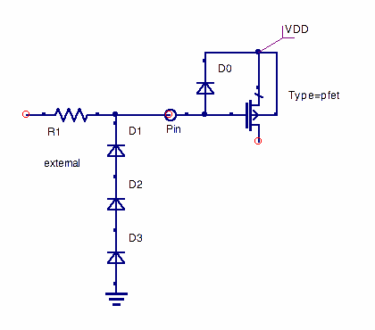
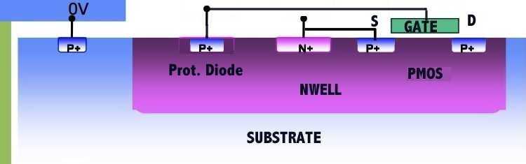
Please suggest me how to connect diodes to avoid Antenna Violation. I referred some books all are explaining it differently, some books suggesting to connect the N(cathode -ntype diffusion) of the diode to metal causing violation and P(anode- p substrate) to GND while some other book suggest to connect P(anode-ptype diffusion) of the diode to the metal causing violation and N(cathode-Nwell) to VDD
 

It does not matter. In fabrication, during metal deposition, a charge may build up on the metal being deposited: this is the Antenna effect. As long as a diffusion area is conncted to that metal line during depositon, the charge will leak out quickly enough such that the voltage does not buold up so far as to destroy something.

Note that "connected to GND" and "connetced to VDD" in your question means directly connected. The "GND" and "VDD" are of no importance, as the antenna effect strikes when the IC has no supply. What is important is that in the first case, the "P" is directly in the P substrate and in the second case the "N" is directly in an n-well.

Slainte!
H.

Hi Slainte,

Thanks for clear explanation. During fabrication this diode doesn't play any role other-than a leakage path for the collected ions but during normal operation will it affect the circuit functionality?What sort of diode we should use if the signal is alternating(AC) and how to connect them?? Please reply.

Thanks
Sam
 

:)))

Slainte is a Scottish greeting :) My name is Hanspi, which is short for Hanspeter.

Regarding diodes: all depends on how much "AC" your signals are. What is VDD, and what is the min and max voltage on the line you want to protect?

Slainte!
Hanspi
 

:)))

Slainte is a Scottish greeting :) My name is Hanspi, which is short for Hanspeter.

Regarding diodes: all depends on how much "AC" your signals are. What is VDD, and what is the min and max voltage on the line you want to protect?

Slainte!
Hanspi

OOps!!! sorry...I dont know Scottish language...whats meaning of Slainte??, hope its not bad..:)
Thanks for the reply. For the layout given to me supply voltage is 1.8V, the antenna violation is occurring in digital section, there I kept a diode with N-connected to the signal and P connected to VSS. Please consider the case when applied signal voltage is alternating between -1.8V to 1.8V(This is my doubt, not there in deign) , how I will connect the diode?.
 

Don't worry, Slainte! simply means "health!"

I assume VDD=1.8V, VSS=0V. Therefore your line can go to -1.8V, approximately three diode voltages below the substrate. Protecting a line whose voltage can go 1.8V below the substrate voltage against antenna effects is no trivial matter at all. It depends on what else is on that line. So two more questions:

1. What is connected to the line? I'm especially interested in hearing whether there are contacts to diffusion areas (SMOS drains, etc) on that line, and of what type they are.

2. What drives the -1.8V on that line? Is that coming from outside the chip, or do you have an isolated region somewhere that is supplied with +-1.8V?

Slainte!
H

Its connected to a gate of the PMOS and alternating signal is coming from outside the chip.

Slainte!
Sam
 

OK, then you obviously don't have ESD diodes on that pad. Would you then have SCRs as ESD structures?

Slainte!
H.
 

The only reason you use a diode, is so you can ignore it
when the circuit is biased normally (diode reverse biased).
If you have a junction-isolated technology the P- substrate
makes a handy common "dump" and the diode is simple as
can be - a N+ contact, in it.
 

Hi Dick! All this is true, but it will still be forward biased when that N+ contact is 1.8V below the substrate, which is what Sam is doing.

What I'm trying to find out with my SCR question is whether Sam already has a leakage path that would prevent a voltage build-up due to antenna effects. If that is inside an SCR, chances are great that the Antenna check will ignore it although it is there.

Slainte!
H

Hi Hanspi & dick_freebird,

Thanks for the response...as mentioned above, its not a problem with my design I am having, its my doubt, How we will protect a transistor in such cases???
 

Hi Sam,

If you go so far below VSS, then the transistor whose gate is connected to that line needs to be a high-voltage transistor. You'd protect that one from an ESD event using SCRs (silicon-controlled rectifiers).

Then you would have that diffusion area you need against antenna charge build-up. The trick then is to go to top metal as close as possible to the gate of that transistor, because during deposition of top metal, when the antenna is really long from the gate to the pad, the diffusion is connected to that line. (By the way, this is also why, in many cases, you don't need an antenna diode at all if you make a bridge to top metal close to the gates of transistors, because in a meaningful circuit, there'll be some diffusion connected to any metal line.)

It may then be that the antenna check rule set will not see that diffusion; SCRs are not simulatable and often black-boxed in DRC/LVS, so you'd need to check by hand and waive the error. If you're lucky, the antenna rule deck is built well and can deal with SCRs.

I hope this general explanation helps! Without a specific situation, it does not make sense to say much more about it. :D

Slainte!
H
 

... How we will protect a transistor in such cases???

I have a different suggestion: An external protection against negative overvoltage with an appropriate current limitation resistor and 3 diodes D1 .. D3 in series to GND:
9003610900_1363712501.gif

which obviously can't be integrated, and a single diode D0 to VDD against positive overvoltage, simultaneously effective against antenna violation, which could be integrated into the very same nwell of the PMOSFET:


Status
Not open for further replies.

Part and Inventory Search

Welcome to EDABoard.com

Sponsor

Back
Top