btv_murthy
Full Member level 3
Dear Sir,
I designed the biasing for the low noise amplifier at Vds=3v, Ids=20mA, need to get the desired s- parameter as follows
f(GHz) s11(dB) S21(dB) S12(dB) S22(dB)
1.3 -1.83312 17.944 -23.083 -10.637
But I am obtaining the following S-parameter values
f(GHz) s11(dB) s21(dB) s12(dB) s22(dB)
1.3 -0.012809 11.721 -86.024 -2.1229
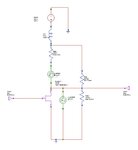
Can anybody help me to get the desired s-parameter low noise amplifier, Here with I am attaching the schematic of the lna
I designed the biasing for the low noise amplifier at Vds=3v, Ids=20mA, need to get the desired s- parameter as follows
f(GHz) s11(dB) S21(dB) S12(dB) S22(dB)
1.3 -1.83312 17.944 -23.083 -10.637
But I am obtaining the following S-parameter values
f(GHz) s11(dB) s21(dB) s12(dB) s22(dB)
1.3 -0.012809 11.721 -86.024 -2.1229
Can anybody help me to get the desired s-parameter low noise amplifier, Here with I am attaching the schematic of the lna