Continue to Site

Welcome to EDAboard.com

Welcome to our site! EDAboard.com is an international Electronics Discussion Forum focused on EDA software, circuits, schematics, books, theory, papers, asic, pld, 8051, DSP, Network, RF, Analog Design, PCB, Service Manuals... and a whole lot more! To participate you need to register. Registration is free. Click here to register now.

Double psu design help

Status
Not open for further replies.

Scolioza

Member level 1
Joined
Mar 5, 2013
Messages
34
Helped
0
Reputation
0
Reaction score
0
Trophy points
1,286
Activity points
1,561
Hello all.
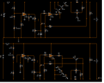
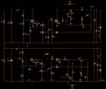
I want to build a double power supply with current limitter only with opamps and transistors. After i read a lot i decided to make my own design (to put in practice what i have learnt by myself ). I simulated the design and it seems to work ok but i do not have experience so i am asking for help in finding any erros or improvements.
I omited the rectifier and filtering part and as a load i used a light bulb .
Thank you in advance
 

Attachments

  • dual.psu.png
    dual.psu.png
    32.1 KB · Views: 65

Hi
The positive regulator at the top looks OK, but there seem to be a couple of mistakes in the negative regulator. Shouldn't the bottom of VR3, C3 and R16 be connected to ground instead of -23V?

Aside from that, I'm wondering if you really need triple Darlingtons for the output. Depending on the maximum output current you want, you may be able to leave out Q3 and Q5, in which case you'd probably want to reduce the value of R5 and R17 as well.

IMHO, it may be a good idea to add resistors from the emitters of Q3, Q5, Q1 and Q6 to ground to ensure some minimum value of current through those transistors when there's little or no load current at the output.

I'd also be more than a bit concerned about high frequency stability. I can't say for sure without building or simulating it, but you may find e.g. that it works fine with a light bulb load but oscilates with a capacitive load.
 
Yep you are right I was in hurry when I redraw the circuit. Here is the circuit you suggested.
Thanks a lot it was very helpful. Now I will try to build it.
Again many thanks.
PS how can I simulate a capacitive load?
 

Attachments

  • psu 2.png
    psu 2.png
    37.7 KB · Views: 49

OK, cool.

I see you've increased R5 and R17 to 4K7 though. I was thinking to reduce the value so the voltage drop isn't too big with high output currents. e.g. If the opamps have to deliver 2mA to the driver transistors, you don't want to drop 10V across those resistors as it would severely limit your maximum output voltage.

OTOH, I suppose you also don't want the opamps to bust a gut when the ouput's shorted and the protection circuitry kicks in, so maybe your original value of 1K is a good compromise after all.

PS how can I simulate a capacitive load?
Just connect a capacitor between one of the outputs and ground. To check for stability, you need to do an AC analysis with an AC signal injected into the circuit somewhere. You'd need to do a number of tests like that with different values of capacitor and different load currents.

Unfortunately, unless your simulator uses very good opamp models, it's probably a waste of time as the sim results won't bear much relation to reality. My vote: just build it and test it.

Some practical tips:
  • Mount the power transistors on a heatsink (with insulating washers and thermal paste).
  • Wish you'd bought flat pack power transistors instead, because the ones you've got are a pain to mount. :razz:
  • Ground the heatsink.
  • Put supply decoupling capacitors on the PCB, close to the power transistors.

P.S. I see you've got more idling current through the driver transistors than the output transistors now. Not a train smash, but it does look a bit odd.
 
Ok. I finally finished building the psu. I works great. Without a propper heatsink i quicky tested for an output current of 1 Amp at 9V at the voltage drop was about 2 mV!!!
But there is one issue that I really dont get it:
On the negative side (always the negative side) if I want to setup an output voltage over -2.55V (eg. -1V) the output drops arround -300mV. On the positive side it works perfectly. I spent 4 hours last night to find the glitch but no luck. Can anyone help me to understand why is that?
PS I tested the circuit with MJ2955 and TIP147 (which i prefer for high hfe) with the same result.
R5 and R17 are 1k5.
Thank you all for helping me.
 

Status
Not open for further replies.

Part and Inventory Search

Welcome to EDABoard.com

Sponsor

Back
Top