Continue to Site

Welcome to EDAboard.com

Welcome to our site! EDAboard.com is an international Electronics Discussion Forum focused on EDA software, circuits, schematics, books, theory, papers, asic, pld, 8051, DSP, Network, RF, Analog Design, PCB, Service Manuals... and a whole lot more! To participate you need to register. Registration is free. Click here to register now.

Output Driver/buffer problem.

Status
Not open for further replies.

fogandflower

Newbie level 5
Joined
Feb 14, 2013
Messages
9
Helped
0
Reputation
0
Reaction score
0
Trophy points
1,281
Activity points
1,342
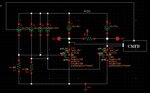
Hi, I have a very simple circuit use pmos source follower as output buffer. The output load is 100ohm resister. The source follower gate voltage difference should define the current go through the load resistor. Design current is 1mA, and expected 100mV single-ended output. However, the test results only showed 50mv output range. I tried a lot simulation condition and could not repeat the test results (always 100mv output). May i know why this happened? What is the root cause?

output.JPG
 

Hi,

you cann't make source follower for differential load in that way. This load resistance making your device asymmetric.
I think that you must enter common mode feedback from output to inputs of current sources, something like this:
SourceFollowerwithFeedback.png
Below shows waveform on which dVin changes from -500m to +500m
Wafeform.png

PS. About CMFB you can read in Razavi's book, section 9.6.
 

hello sarge,

actually i have common mode feedback circuit. The common mode is well controlled. The circuit is work perfectly except the output range. That's why i only draw the output driver part.
 

You have CMFB in your output driver or in other place? Can you draw a more detailed schematic?

I meant, that you can place CMFB circuit in your output buffer and I drawed similar output driver, only with nmos transistors.
In any case, more detailed schematic will give for all us more information .
 

Hello Sarge,

Please check the new attachment.

current source I1 and I2 are output current bias,
I4/I5 is cmfb current bias
I6/I7 is current bias based on digital code.

So when the code is changing, different current will go through resistor R1&R2, this will cause gate voltage change of M32/M33. Since M32/M33 are source follower, we are expecting OP/ON will see the same voltage change.
 

Attachments

  • output2.JPG
    output2.JPG
    80.1 KB · Views: 57

How do you determine what your CMFB circuit working properly?

Can you try to apply cmfb to the I1/I2 current sources(as I suggested earlier)?
 

How do you determine what your CMFB circuit working properly?

Can you try to apply cmfb to the I1/I2 current sources(as I suggested earlier)?

Hello Sarge

Design common mode is 0.8V, measure result is 0.798, and the output signal is quite stable. And the output common mode change will change the current go through R1/R2, it will cause gate voltage M32/M33 change as well.
 

Do you shure that dVin on gates M32/M33 is changes on adequate value? For example, in my test circuit, for dVout = 100 mV i need dVin = 170mV.
 

Hello Sarge,

In the design, i need about 140mv change on M32/M33 to get output 100mv. Worst case output is about 90mv. However, test results only 50mv.
 

In the design, i need about 140mv change on M32/M33 to get output 100mv.
As I understand, this are theoretical values, which you got after calculations. I think, that you will need to find such value of dVin, that dVout = 100mV in simulation, and then rebuild your CMFB circuit.

pmos source follower with 100 Ohm load resistance:
SourceFollowerPmos.png

As you can seen, in that case dVin = 170 mV also. Be carefull with proper choise dimension of transistors and voltages.

ps. connect body terminals of transistor to vdd.
 

As I understand, this are theoretical values, which you got after calculations. I think, that you will need to find such value of dVin, that dVout = 100mV in simulation, and then rebuild your CMFB circuit.

pmos source follower with 100 Ohm load resistance:
View attachment 87638

As you can seen, in that case dVin = 170 mV also. Be carefull with proper choise dimension of transistors and voltages.

ps. connect body terminals of transistor to vdd.

Hello Sarge,

150mv dvin got 100mv output is based on simulation results. Why you mentioned the output source follower body should connect to vdd instead of source?
 

Why you mentioned the output source follower body should connect to vdd instead of source?

Hi,
I think, because if it doesn't connect to vdd, then value Vth is changed.
 

Status
Not open for further replies.

Part and Inventory Search

Welcome to EDABoard.com

Sponsor

Back
Top